

NSC LMS202EIMW, LMS202ECMX, LMS202ECMWX, LMS202ECMW, LMS202ECM Datasheet
...
LMS202E
15KV ESD Rated, 5V Single Supply TIA/EIA-232 Dual
Transceivers
LMS202E 15KV ESD Rated, 5V Single Supply TIA/EIA-232 Dual Transceivers
March 2003
General Description
The LMS202E features two transmitters and two receivers
for RS-232 communication. It has a DC-to-DC converter that
permits the device to operate with only a single +5V power
supply. The on-chip DC-to-DC converter which utilizes four
external 0.1µF capacitors to generate dual internal power
supplies for RS-232 compatible output levels.
The device meet EIA/TIA-232E and CCITT V.28 specifications up to 230kbits/sec. The LMS202E is available in a 16
pin narrow and wide SOIC package.
±
The transmitter outputs and receiver inputs have
electrostatic discharge (ESD) protection. The LMS202E survives a
pins when subjected according to Human Body Model or IEC
1000-4-2 (EN61000-4-2),air-gap specification. It survives a
±
4-2), contact specification. This device is designed for use in
harsh environments where ESD is a concern.
±
15kV ESD event to the RS-232 input and output
8kV discharge when subjected to IEC 1000-4-2 (EN61000-
15kV
Features
n ESD protection for RS-232 I/O pins
n Single +5V power supply
n 230 kbps data rate
n On-board DC-to-DC converter
n 0.1µF charge pump capacitors
n Drop-in replacement to Maxim’s MAX202E
Applications
n POS equipment (Bar code reader)
n Hand-held equipment
n General purpose RS-232 communication
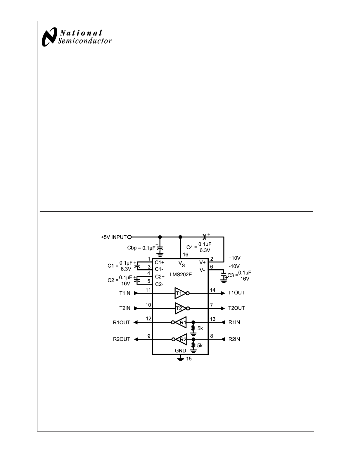
Connection Diagram and Typical Circuit
±
15kV-IEC1000 4-2 (EN61000-4-2) Contact
—
Discharge
±
8kV-IEC1000 4-2 (EN61000-4-2) Air-Gap Discharge
—
±
15kV Human Body Model
—
20048001
© 2003 National Semiconductor Corporation DS200480 www.national.com
Pin Descriptions
Pin Number Pin Name Pin Function
LMS202E
1, 3 C1+, C1− External capacitor connection pins. Recommended external capacitor C1 = 0.1µF (6.3V)
2 V+ Positive supply for TIA/EIA-232E drivers. Recommended external capacitor C4 = 0.1µF (6.3V)
4, 5 C2+, C2− External capacitor connection pins. Recommended external capacitor C2 = 0.1µF (16V)
6 V− Negative supply for TIA/EIA-232E drivers. Recommended external capacitor C3 = 0.1µF (16V)
7, 14 T1out, T2out Transmitter output pins conform to TIA/EIA-232E levels. The typical transmitter output swing is
±
8V when loaded 3kΩ load to ground. The open-circuit output voltage swings from (V+ − 0.6V)
to V−
8,13 R1in, R2in Receiver inputs accept TIA/EIA-232
9, 12 R1out and R2out Receiver output pins are TTL/CMOS compatible
10, 11 Tin1, Tin2 Transmitter input pins are TTL/CMOS compatible. Inputs of transmitter do not have pull-up
resistors. Connect all unused transmitter inputs to ground
15 GND Ground pin
16 V
S
Power supply pin for the device, +5V (±10%)
Ordering Information
Package Part Number Package Marking Transport Media NSC Drawing
16-Pin SOIC
16-Pin Wide SOIC
LMS202ECM
LMS202ECMX 2.5k Units Tape and Reel
LMS202EIM
LMS202EIMX 2.5k Units Tape and Reel
LMS202ECMW
LMS202ECMWX 1.0k Units Tape and Reel
LMS202EIMW
LMS202EIMWX 1.0k Units Tape and Reel
LMS202ECM
LMS202EIM
LMS202ECMW
LMS202EIMW
48 Units/Rail
48 Units/Rail
45 Units/Rail
45 Units/Rail
M16A
M16B
www.national.com 2
LMS202E
Absolute Maximum Ratings (Note 1)
If Military/Aerospace specified devices are required,
please contact the National Semiconductor Sales Office/
Distributors for availability and specifications.
V
S
V+ (V
V− +0.3V to −14V
Driver Input Voltage, T
IN
Receiver Input Voltage, R
Driver Output Voltage T
O
Receiver Output Voltage R
Short Circuit Duration, T
O
IN
O
−0.3V to (V+ +0.3V)
(V− −0.3V to (V+ + 0.3V)
ESD Rating
IEC 1000-4-2) (Note 7)
(Note 8)
Air-Gap Discharge 15kV
Contact Discharge 8kV
Human Body Model (Note 2)
−0.3V to 6V
− 0.3V) to + 14V
S
±
−0.3 to (VS+ 0.3)
Continuous
30V
(Note 9) 2kV
ESD Rating (MM) 200V (Note 6) (Note 9)
Soldering Information
Infrared or Convection 235˚C
(20sec.)
Junction Temperature 150˚C
Storage Temperature Range −65˚C to +150˚C
Operating Ratings
Supply Voltage V
Ambient Temperature Range, T
S
A
Commercial (C) 0˚C to +70˚C
Industrial (I) −40˚C to +85˚C
Package Thermal Resistance
(Note 3)
SO 71˚C/W
WSO 55˚C/W
4.5V to 5.5V
(Note 8) 15kV
Electrical Characteristics
Over recommended operating supply and temperature ranges unless otherwise specified C1 = C2 = C3 = C4 = Cbp = 0.1µF
Symbol Parameter Conditions Min
(Note 5)
DC Characteristics
I
S
Supply Current No Load, TA= 25˚C 1 7 mA
Logic
I
INPUT
V
THL
V
THH
V
OL
Input Leakage Current TIN=0VtoV
Input Logic Theshold Low T
Input Logic Theshold High T
TTL/CMOS Output Voltage
IN
IN
R
OUT,IOUT
= 3.2mA 0.4 V
S
Low
V
OH
TTL/CMOS Output Voltage
R
OUT,IOUT
= −1.0mA 3.5 VS−0.1 V
High
RS-232 Receiver Inputs
V
RI
Receiver Input Voltage
Range
V
RTHL
Receiver Input Theshold
VS= 5V, TA= 25˚C 0.8 1.4 V
Low
V
RTHH
Receiver Input Theshold
VS= 5V, TA= 25˚C 2 2.4 V
High
V
R
HYST
I
Receiver Input Hysteresis VS= 5V 0.2 0.6 1.0 V
Receiver Input Resistance VS= 5V, TA= 25˚C 3 5 7 kΩ
RS-232 Transmitter Outputs
V
O
Transmitter Output Voltage
All transmitters loaded with 3kΩ to GND
Swing
R
O
I
OS
Output Resistance VS=V+=V−=0V,
=±2V
V
O
Output Short Circuit Current
Timing Characteristics
DR Maximum Data Rate C
= 50pF to 1000pF,
L
=3kΩ to 7kΩ
R
L
2.0 V
−30 +30 V
±
5
300 Ω
230 kbps
Typ Max
(Note 5)
±
10 µA
0.8 V
±
8V
±
11
±
60 mA
Units
www.national.com3
 Loading...