

NSC LM4121IM5X-ADJ, LM4121IM5X-1.2, LM4121IM5-1.2, LM4121AIM5X-ADJ, LM4121AIM5X-1.2 Datasheet
...
April 2000
LM4121
Precision Micropower Low Dropout Voltage Reference
LM4121 Precision Micropower Low Dropout Voltage Reference
General Description
The LM4121 is a precision bandgap voltage reference available in a fixed 1.25V and adjustable version with up to 5 mA
current source and sink capability.
This series reference operates with input voltages as low as
1.8V and up to 12Vconsuming 160 µA (Typ.) supply current.
In power down mode, device current drops to less than 2 µA.
The LM4121 comes in two grades A and Standard. The best
grade devices (A) have an initial accuracy of 0.2%, while the
standard have an initial accuracy of 0.5%, both with a
tempco of 50ppm/˚C guaranteed from −40˚C to +125˚C.
The very low operating voltage, low supply current and
power-down capability of the LM4121 makes this product an
ideal choice for battery powered and portable applications.
The device performance is guaranteed over the industrial
temperature range (−40˚C to +85˚C), while certain specs are
guaranteed over the extended temperature range (−40˚C to
+125˚C). Please contact National for full specifications over
the extended temperature range. The LM4121 is available in
a standard 5-pin SOT-23 package.
Features (LM4121-1.2)
n Small SOT23-5 package
n Low voltage operation
n High output voltage accuracy: 0.2%
n Source and Sink current output:
n Supply current: 160 µA Typ.
n Low Temperature Coefficient: 50 ppm/˚C
n Enable pin
n Output voltages: 1.25V and Adjustable
n Industrial temperature Range: −40˚C to +85˚C
n (For extended temperature range, −40˚C to 125˚C,
contact National Semiconductor)
±
5mA
Applications
n Portable, battery powered equipment
n Instrumentation and process control
n Automotive & Industrial
n Test equipment
n Data acquisition systems
n Precision regulators
n Battery chargers
n Base stations
n Communications
n Medical equipment
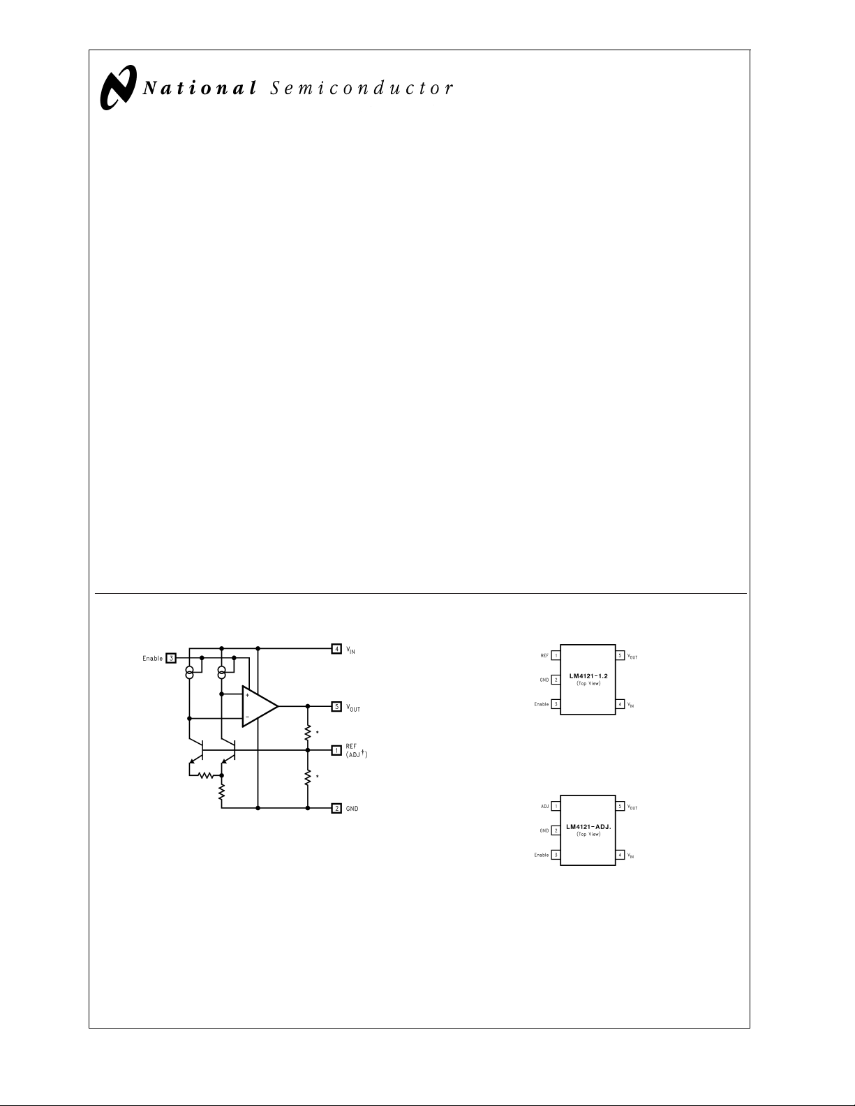
LM4121-1.2 Block Diagram
*
Resistors are removed on the LM4121-ADJ
†
LM4121-ADJ only
DS101291-1
Connection Diagram
DS101291-2
Refer to the Ordering Information Table in this Data Sheet for Specific
Part Number
SOT23-5 Surface Mount Package
DS101291-35
© 2000 National Semiconductor Corporation DS101291 www.national.com
Ordering Information
LM4121
Industrial Temperature Range (−40˚C to + 85˚C)
Initial Output Voltage Accuracy at 25˚C
And Temperature Coefficient
0.2%, 50 ppm/˚C max (A grade)
0.5%, 50 ppm/˚C max
LM4121 Supplied as
1000 Units, Tape and
Reel
LM4121AIM5-1.2 LM4121AIM5X-1.2 R19A
LM4121AIM5-ADJ LM4121AIM5X-ADJ R20A
LM4121IM5-1.2 LM4121IM5X-1.2 R19B
LM4121IM5-ADJ LM4121IM5X-ADJ R20B
SOT-23 Package Marking Information
Only four fields of marking are possible on the SOT-23’s small surface. This
table gives the meaning of the four fields.
Field Information
First Field:
R = Reference
Second and third Field:
19 = 1.250V Voltage Option
20 = Adjustable
Fourth Field:
A-B = Initial Reference Voltage Tolerance
±
A=
0.2%
±
B=
0.5%
LM4121 Supplied as
3000 Units, Tape and
Reel
Top
Marking
www.national.com 2
LM4121
Absolute Maximum Ratings (Note 1)
If Military/Aerospace specified devices are required,
please contact the National Semiconductor Sales Office/
Distributors for availability and specifications.
Lead Temperature:
Soldering, (10 sec.) +260˚C
Vapor Phase (60 sec.) +215˚C
Infrared (15 sec.) +220˚C
Maximum Voltage on input or
enable pins −0.3V to 14V
Output Short-Circuit Duration Indefinite
Power Dissipation (T
MA05B package − θ
= 25˚C) (Note 2):
A
JA
280˚C/W
Operating Range (Note 1)
Storage Temperature Range −65˚C to +150˚C
Ambient Temperature Range −40˚C to +85˚C
Junction Temperature Range −40˚C to +125˚C
Power Dissipation 350 mW
ESD Susceptibility (Note 3)
Human Body Model
Machine Model
2kV
200V
Electrical Characteristics
LM4121-1.250V
standard typeface are for T
Symbol Parameter Conditions Min (Note 5) Typ (Note 4) Max (Note 5) Units
V
OUT
TCV
∆V
∆V
Min-V
V
I
I
V
V
I
I
I
/˚C Temperature Coefficient −40˚C ≤ TA≤ +125˚C 14 50 ppm/˚c
OUT
/∆V
OUT
/∆I
OUT
IN
N
S
SS
H
L
H
L
SC
Hyst Thermal Hysteresis
∆V
OUT
Output Voltage Initial
Accuracy
LM4121A-1.250
LM4121-1.250
Line Regulation 1.8V ≤ VIN≤ 12V 0.0007 0.009
IN
Load Regulation
LOAD
Minimum Operating Voltage I
Output Noise Voltage 0.1 Hz to 10 Hz 20 µV
Supply Current 160 250
Power-down Supply Current VIN= 12V
Logic High Input Voltage 1.6 1.5 V
Logic Low Input Voltage 0.4 V
Logic High Input Current 7 15 µA
Logic Low Input Current 0.1 µA
Short Circuit Current
(Note 8)
Long Term Stability
(Note 9)
Unless otherwise specified VIN= 3.3V, I
= 25˚C, and limits in boldface type apply over the −40˚C ≤ TA≤ +85˚C temperature range.
j
LOAD
=0,C
= 0.01µF, TA=Tj= 25˚C. Limits with
OUT
1.250
±
0.2
±
0.5
0.012
0mA≤I
≤ 1 mA 0.03 0.08
LOAD
0.17
1mA≤I
≤ 5 mA 0.01 0.04
LOAD
0.1
−1 mA ≤ I
−5 mA ≤ I
= 5mA 1.5 1.8 V
LOAD
≤ 0 mA 0.04 0.12
LOAD
≤ −1 mA 0.01
LOAD
10 Hz to 10 kHz 30 µV
275
Enable = 0.4V
Enable = 0.2V
1
2
0.2
V
IN
= 3.3V, V
=0 15
OUT
630
V
= 12V, V
IN
=0 17
OUT
630
−40˚C ≤ T
≤ 125˚C 0.5 mV/V
A
1000 hrs.@25˚C 100 ppm
%
%/V
%/mA
PP
RMS
µA
µA
mA
www.national.com3
Electrical Characteristics
LM4121-ADJ
LM4121
its with standard typeface are for T
range.
Symbol Parameter Conditions Min (Note 5) Typ (Note 4) Max (Note 5) Units
V
OUT=VREF
TCV
/˚C Temperature Coefficient −40˚C ≤ TA≤ +125˚C 14 50 ppm/˚c
REF
∆V
/∆V
REF
IN
∆V
/∆I
OUT
LOAD
Min-V
IN
V
N
I
S
I
SS
I
BIAS
V
H
V
L
I
H
I
L
I
SC
Hyst Thermal Hysteresis
∆V
OUT
Note 1: “Absolute Maximum Ratings” indicate limits beyond which damage to the device may occur. Operating Ratings indicate conditions for which the device is
intended to befunctional,butdonotguaranteespecific performance limits. For guaranteed specifications and test conditions, see Electrical Characteristics. The guaranteed specifications apply only for the test conditions listed. Some performance characteristics may degrade when the device is not operated under the listed test
conditions.
Note 2: WithoutPCB copper enhancements. The maximum power dissipation must be de-rated at elevated temperatures and is limited by T
temperature), θ
−TA)/θ
J-A
Note 3: The human body model is a 100 pF capacitor discharged through a 1.5 kΩ resistor into each pin. The machine model is a 200 pF capacitor discharged di-
rectly into each pin.
Note 4: Typical numbers are at 25˚C and represent the most likely parametric norm.
Note 5: Limitsare 100% production tested at 25˚C. Limits over the operating temperature range are guaranteed through correlation using Statistical Quality Control
(SQC) methods. The limits are used to calculate National’s Averaging Outgoing Quality Level (AOQL).
Note 6: Output noise for 1.25V option. Noise is proportional to V
Note 7: Bias Current flows out of the Adjust pin.
Note 8: Thermal hysteresis is defined as the change in +25˚C output voltage before and after exposing the device to temperature extremes.
Note 9: Long term stability is change in V
(junction to ambient thermal resistance) and TA(ambient temperature). The maximum power dissipation at any temperature is: PDiss
J-A
up to the value listed in the Absolute Maximum Ratings.
Unless otherwise specified VIN= 3.3V, V
= 25˚C, and limits in boldface type apply over the −40˚C ≤ TA≤ +85˚C temperature
j
OUT=VREF,ILOAD
=0,C
= 0.01µF, TA=Tj= 25˚C. Lim-
OUT
Output Voltage Initial
±
Accuracy
1.216
0.2
LM4121A-ADJ
LM4121-ADJ
±
0.5
Line Regulation 1.8V ≤ VIN≤ 12V 0.0007 0.009
0.012
0mA≤I
≤ 1 mA 0.03 0.08
LOAD
0.17
Load Regulation
Minimum Operating Voltage I
1mA≤I
−1 mA ≤ I
−5 mA ≤ I
=5mA 1.5 1.8 V
LOAD
≤ 5 mA 0.01 0.04
LOAD
≤ 0 mA 0.04 0.12
LOAD
≤ −1 mA 0.01
LOAD
0.1
Output Noise Voltage (Note 6) 0.1 Hz to 10 Hz 20 µV
10 Hz to 10 kHz 30 µV
Supply Current 160 250
275
Power-down Supply Current VIN= 12V
Enable = 0.4V
Enable = 0.2V
1
2
Reference Pin Bias Current (Note 7) 15 40 nA
Logic High Input Voltage 1.6 1.5 V
Logic Low Input Voltage 0.4 V
0.2
Logic High Input Current 7 15 µA
Logic Low Input Current 0.1 µA
=0 15
V
OUT
Short Circuit Current
V
= 12V, V
IN
=0 17
OUT
630
630
−40˚C ≤ T
≤ 125˚C 0.5 mV/V
A
(Note 8)
Long Term Stability
1000 hrs.@25˚C 100 ppm
(Note 9)
(maximum junction
JMAX
.
OUT
at 25˚C measured continuously during 1000 hrs.
REF
MAX
=(T
%
%/V
%/mA
PP
RMS
µA
µA
mA
JMAX
www.national.com 4
LM4121
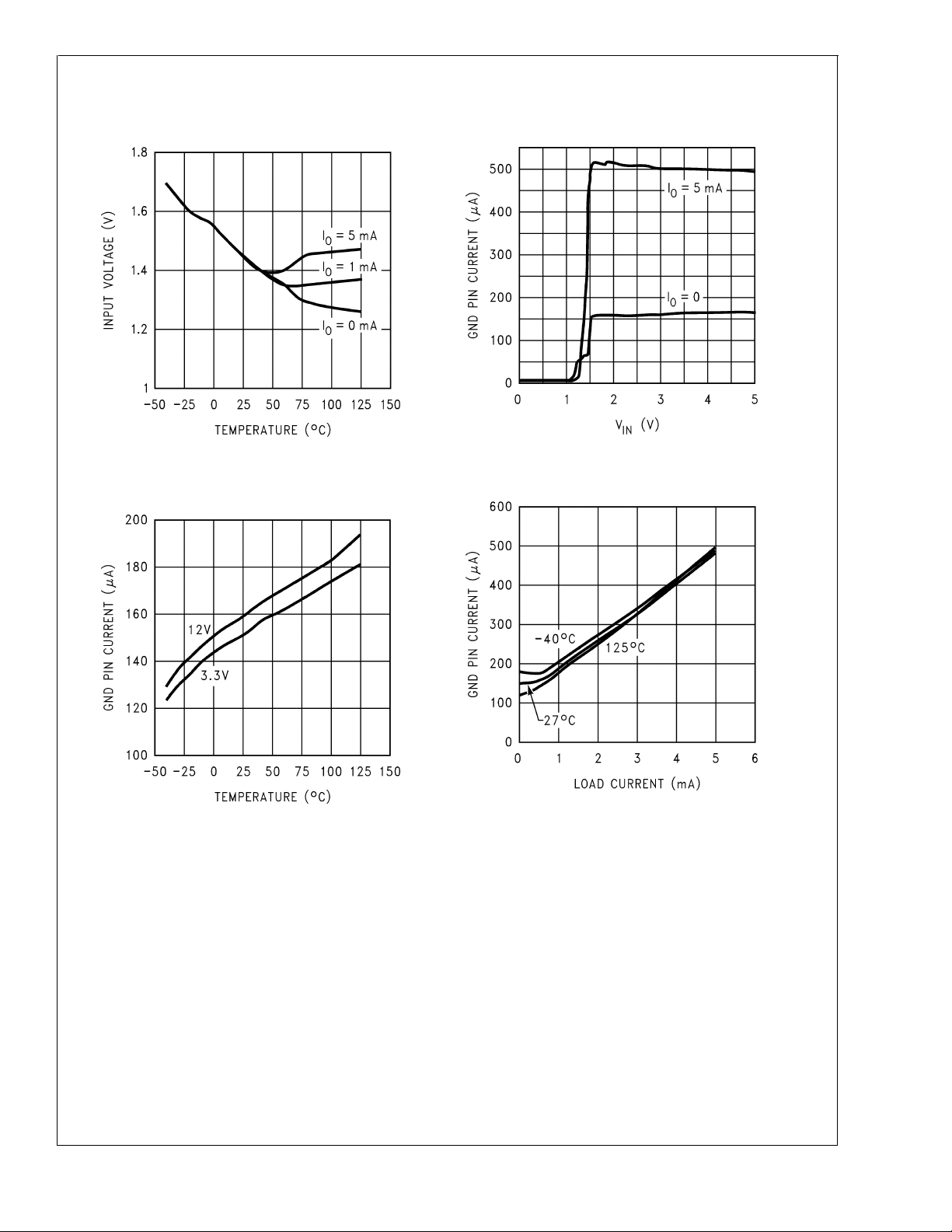
LM4121- (All Options) Typical Operating Characteristics Unless otherwise specified, V
= 3.3V, V
Minimum Input Voltage vs Temperature
GND Pin Current at No Load
vs Temperature
OUT
= 1.25V, I
LOAD
=0,C
= 0.022µF, TA= 25˚C and VEN=VIN.
OUT
GND Pin Current vs V
DS101291-12
GND Pin Current vs Load
IN
DS101291-13
IN
DS101291-14
DS101291-15
www.national.com5
 Loading...