

NSC LM3677TL-1.8EV Datasheet
LM3677 Evaluation Board
National Semiconductor
Application Note 1595
Jingdong Chen
March 2007
Introduction
The LM3677 evaluation board is a working demonstration of
a step down DC-DC converter. This application note contains
information about the evaluation board. For further information on buck converter topology, device electrical characteristics, and component selection please refer to the datasheet.
General Description
The LM3677 converts high input voltages to lower output voltages with high efficiency through an inductor based switching
topology. Automatic intelligent switching between PWM lownoise and PFM low-current mode offers improved system
control. LM3677 is available in both fixed output voltage options and adjustable voltage options range from 1.2V to 3.3V
in a micro SMD-5 package. The fixed output voltage options
available in a SMD-5 package are 1.2V, 1.3V, 1.5V, 1.6V,
1.8V, 2.5V, 2.8V, and 3.3V.
Operating Conditions
•
Recommended input voltage range:
VIN = 2.7V to 4.5V for 1.1V ≤ V
OUT
< 1.5V
VIN = 2.7V to 5.5V for 1.5V ≤ V
OUT
< 1.8V
VIN = (V
OUT
+ V
DROPOUT
) to 5.5V for 1.8V ≤ V
OUT
≤ 3.3V
where V
DROPOUT
= I
LOAD
* (R
DSON, PFET
+ R
INDUCTOR
)
•
Recommended load current: 0 mA ≤ I
OUT
≤ 600 mA
•
Ambient temperature (TA) range: -30C to +85C
•
Junction temperature (TJ) range: -30C to +125C
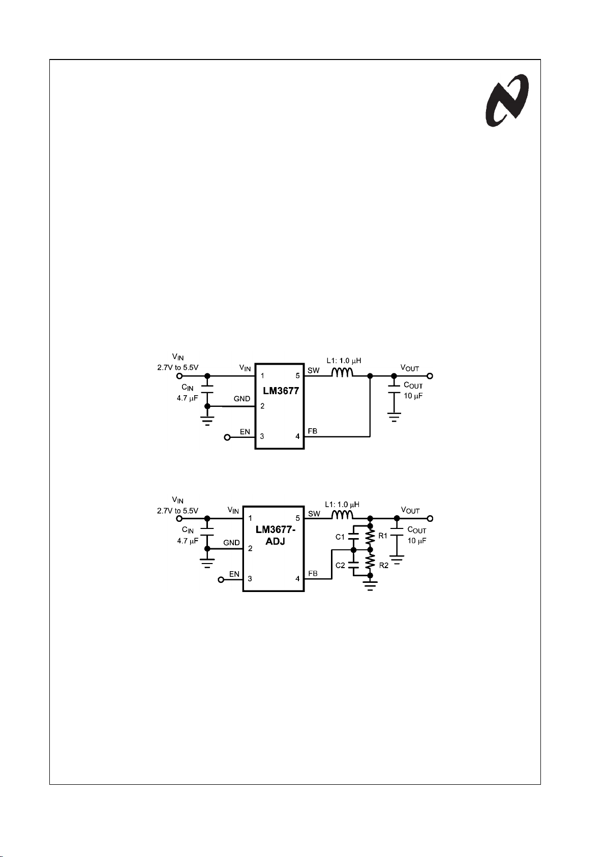
Typical Application
30012025
FIGURE 1. Fixed Output Voltage--Typical Application Circuit
30012026
FIGURE 2. Adjustable Output Voltage—Typical Application Circuit
© 2007 National Semiconductor Corporation 300120 www.national.com
LM3677 Evaluation Board AN-1595
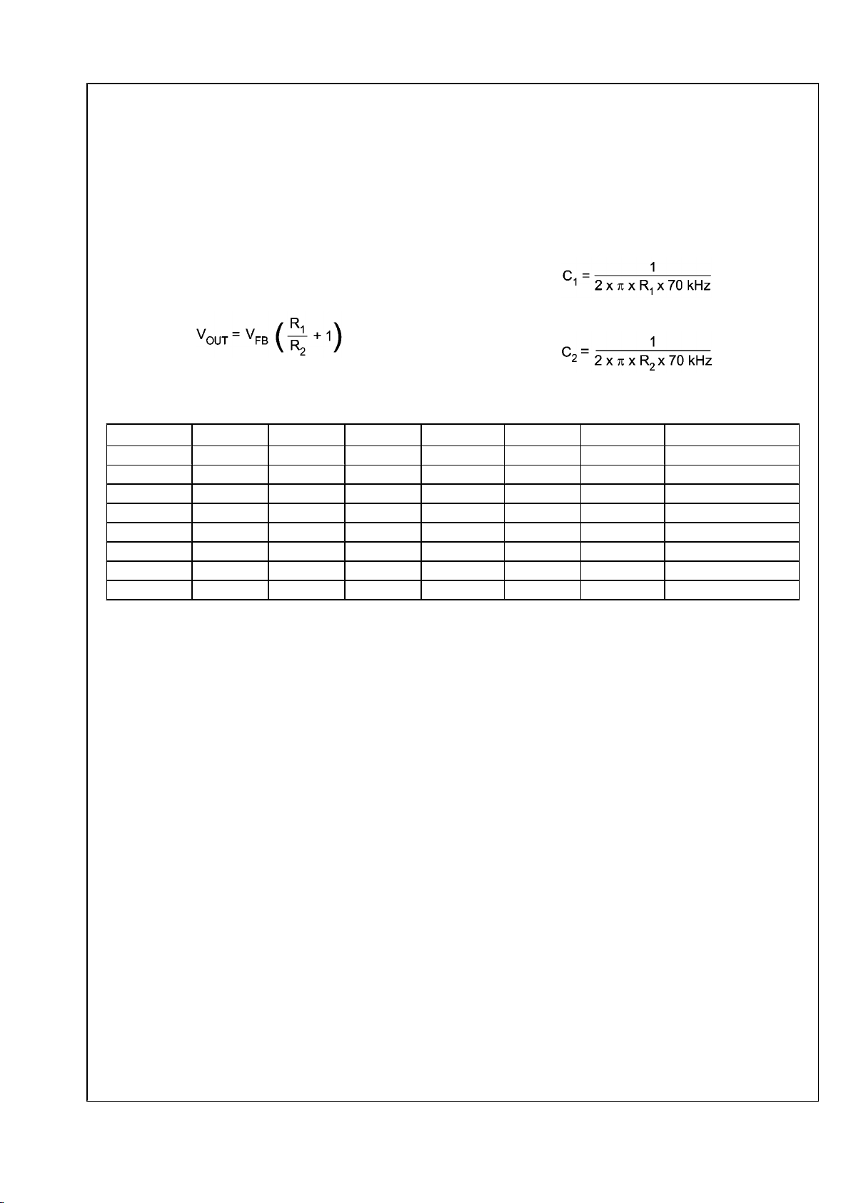
Output Voltage Selection for
LM3677TL-ADJ
The output voltage of the adjustable parts can be programmed through the resistor network connected from V
OUT
to FB to GND. The resistor from FB to GND (R2) should be
200kΩ to keep the current drawn throught this network well
below 16µA quiescent current level (PFM mode) but large
enough that it is not susceptible to noise. If R2 is 200kΩ, and
given the VFB is 0.5V, then the current through the resistor
feedback network will be 2.5µA. The ouput voltage of the adjustable parts ranges from 1.2V to 3.3V. The output voltage
formula is:
V
OUT
: output voltage (V)
VFB: feedback voltage (0.5V typical)
R1: feedback resistor from V
OUT
to FB(Ω )
R2: feedback resistor from FB to GND (Ω)
For the fixed output voltage parts the feedback resistors are
internal and R1 is 0Ω.
The bypass capacitors C1and C2 (labeled C3 and C4 on Eval-
uation Board) in parallel with the feedback resistors are chosen for increased stability. Below are the formulas for C1and
C2.
Table1. LM3677-ADJ Configurations for Various V
out
(Circuit of Figure 2)
V
OUT
(V)
R1(kΩ ) R2(kΩ )
C1(pF) C2(pF) L (µH) CIN (µF) C
OUT
(µF)
1.2 280 200 8.2 none 1.0 4.7 10
1.3 320 200 8.2 none 1.0 4.7 10
1.5 357 178 6.8 none 1.0 4.7 10
1.6 442 200 5.6 none 1.0 4.7 10
1.8 464 178 5.6 none 1.0 4.7 10
2.5 402 100 6.0 none 1.0 4.7 10
2.8 464 100 5.6 24 1.0 4.7 10
3.3 562 100 5.6 24 1.0 4.7 10
www.national.com 2
AN-1595
 Loading...