

NSC LM3677, LM3677TLX-2.5 Datasheet
March 2007
LM3677
3MHz, 600mA Miniature Step-Down DC-DC Converter for
Ultra Low Voltage Circuits
General Description
The LM3677 step-down DC-DC converter is optimized for
powering ultra-low voltage circuits from a single Li-Ion cell
battery and input voltage rails from 2.7V to 5.5V. It provides
up to 600mA load current, over the entire input voltage range.
The LM3677 is configured to four output voltages of 1.3V,
1.5V, 1.8V and 2.5V.
The device offers superior features and performance for mo-
bile phones and similar portable applications with complex
power management systems. Automatic intelligent switching
between PWM low-noise and PFM low-current mode offers
improved system control. During PWM mode operation, the
device operates at a fixed-frequency of 3 MHz (typ). PWM
mode drives loads from ~ 80mA to 600mA max. Hysteretic
PFM mode extends the battery life by reducing the quiescent
current to 16 µA (typ) during light load and standby operation.
Internal synchronous rectification provides high efficiency. In
shutdown mode (Enable pin pulled down), the device turns
off and reduces battery consumption to 0.01 µA (typ).
The LM3677 is available in a lead-free (NO PB) 5-bump micro
SMD package. A switching frequency of 3 MHz (typ) allows
use of tiny surface-mount components. Only three external
surface-mount components, an inductor and two ceramic capacitors, are required.
Features
■
16 µA typical quiescent current
■
600 mA maximum load capability
■
3 MHz PWM fixed switching frequency (typ)
■
Automatic PFM/PWM mode switching
■
Available in 5-bump micro SMD package
■
Internal synchronous rectification for high efficiency
■
Internal soft start
■
0.01 µA typical shutdown current
■
Operates from a single Li-Ion cell battery
■
Only three tiny surface-mount external components
required (solution size less than 20 mm2)
■
Current overload and Thermal shutdown protection
Applications
■
Mobile phones
■
PDAs
■
MP3 players
■
W-LAN
■
Portable Instruments
■
Digital still cameras
■
Portable Hard disk drives
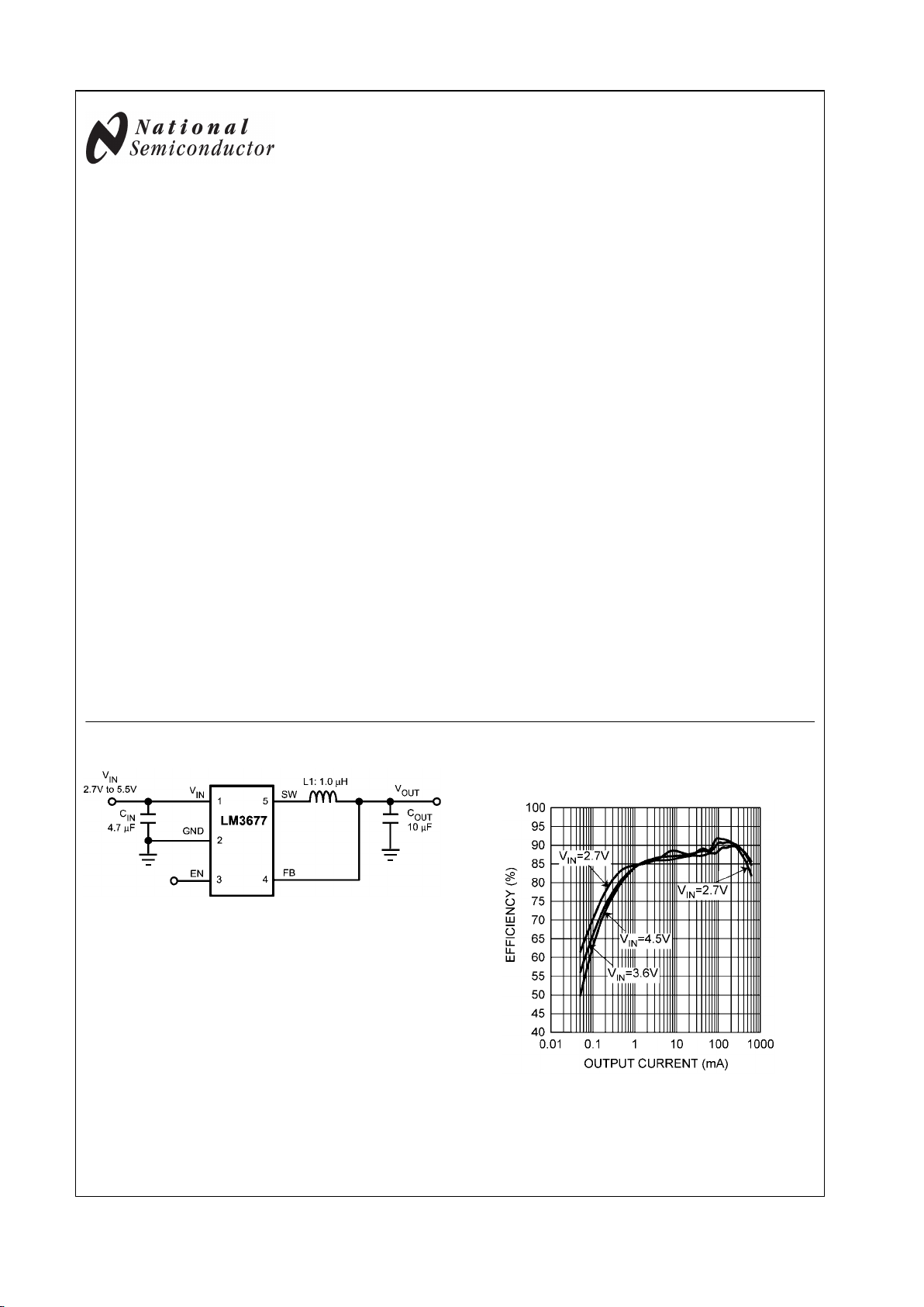
Typical Application Circuit
30008401
FIGURE 1. Typical Application Circuit
Efficiency vs. Output Current
(V
OUT
= 1.8V)
30008487
© 2007 National Semiconductor Corporation 300084 www.national.com
LM3677 3MHz, 600mA Miniature Step-Down DC-DC Converter for Ultra Low Voltage Circuits
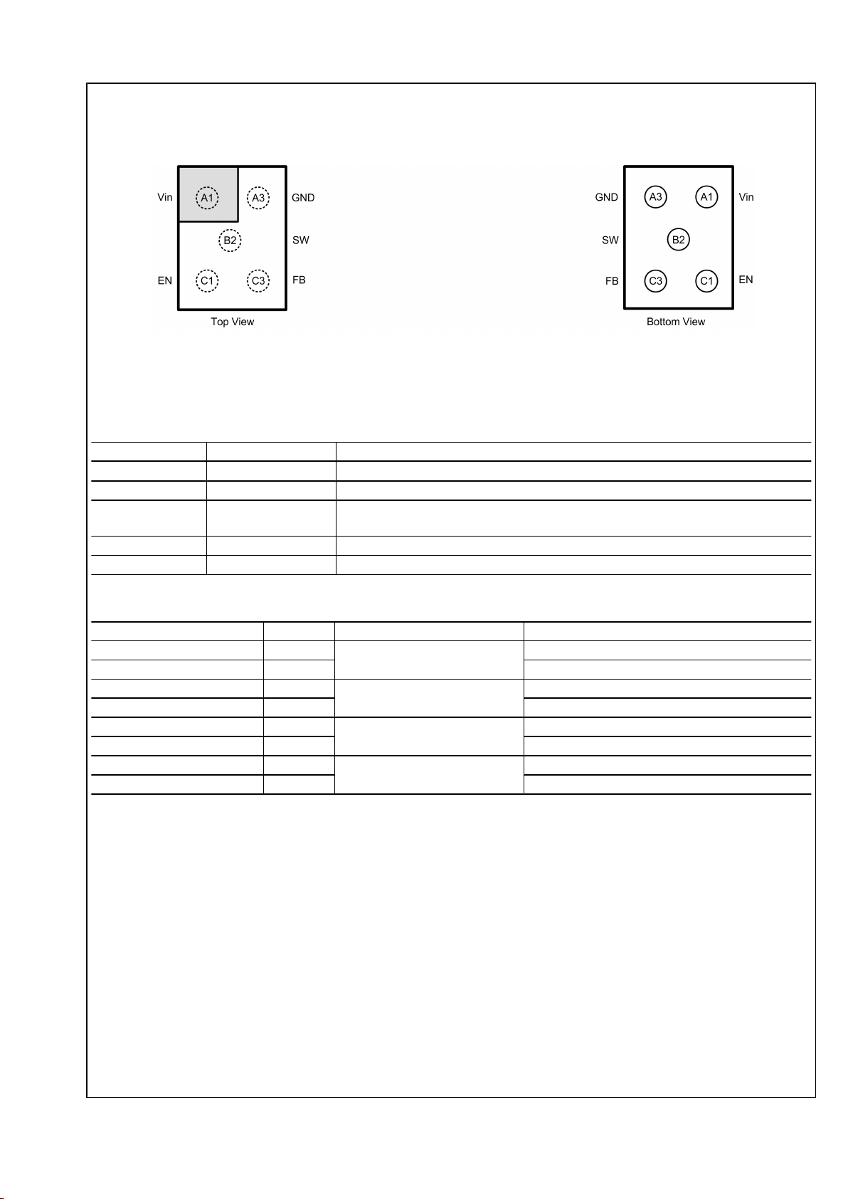
Connection Diagram and Package Mark Information
5-Bump micro SMD Package NS Package Number TLA05FEA
30008444
FIGURE 2. 5 Bump Micro SMD Package
Pin Descriptions
Pin # Name Description
A1 V
IN
Power supply input. Connect to the input filter capacitor (Figure 1).
A3 GND Ground pin.
C1 EN Enable pin. The device is in shutdown mode when voltage to this pin is <0.4V and enabled
when >1.0V. Do not leave this pin floating.
C3 FB Feedback analog input. Connect directly to the output filter capacitor ( FIGURE 1).
B2 SW Switching node connection to the internal PFET switch and NFET synchronous rectifier.
Ordering Information
Order Number Spec Package Marking Supplied As
LM3677TL-1.3 NOPB
V
250 units, Tape-and-Reel
LM3677TLX-1.3 NOPB 3000 units, Tape-and-Reel
LM3677TL-1.5 NOPB
X
250 units, Tape-and-Reel
LM3677TLX-1.5 NOPB 3000 units, Tape-and-Reel
LM3677TL-1.8 NOPB
Y
250 units, Tape-and-Reel
LM3677TLX-1.8 NOPB 3000 units, Tape-and-Reel
LM3677TL-2.5 NOPB
Z
250 units, Tape-and-Reel
LM3677TLX-2.5 NOPB 3000 units, Tape-and-Reel
Note: 1.2V, 1.6V, 2.8V and ADJ are coming soon.
www.national.com 2
LM3677
Absolute Maximum Ratings (Note 1)
If Military/Aerospace specified devices are required,
please contact the National Semiconductor Sales Office/
Distributors for availability and specifications.
If Military/Aerospace specified devices are required, please
contact the National Semiconductor Sales Office/Distributors
for availability and specifications.
VIN Pin: Voltage to GND −0.2V to 6.0V
FB, SW, EN Pin: (GND−0.2V) to
(VIN + 0.2V)
Continuous Power Dissipation
(Note 3)
Internally Limited
Junction Temperature (T
J-MAX
) +125°C
Storage Temperature Range −65°C to +150°C
Maximum Lead Temperature
(Soldering, 10 sec.)
260°C
ESD Rating (Note 4)
Human Body Model: All Pins 2.0 kV
Machine Model: All Pins 200V
Operating Ratings (Note 1), (Note 2)
Input Voltage Range 2.7V to 5.5V
Recommended Load Current 0mA to 600 mA
Junction Temperature (TJ) Range −30°C to +125°C
Ambient Temperature (TA) Range (Note5)−30°C to +85°C
Thermal Properties
Junction-to-Ambient Thermal
Resistance (θJA) (Note 6)
85°C/W
Electrical Characteristics (Note 2), (Note 8), (Note 9) Limits in standard typeface are for T
J
= TA = 25°C.
Limits in boldface type apply over the operating ambient temperature range (−30°C ≤ TA ≤ +85°C). Unless otherwise noted,
specifications apply to the LM3677 with VIN = EN = 3.6V.
Symbol Parameter Condition Min Typ Max Units
V
IN
Input Voltage 2.7 5.5 V
V
FB
Feedback Voltage PWM mode -2.5 +2.5 %
V
REF
Internal Reference Voltage 0.5 V
I
SHDN
Shutdown Supply Current EN = 0V 0.01 1 µA
I
Q
DC Bias Current into V
IN
No load, device is not switching 16 35 µA
R
DSON (P)
Pin-Pin Resistance for PFET VIN= VGS= 3.6V, ISW= 100mA 350 450
mΩ
R
DSON (N)
Pin-Pin Resistance for NFET VIN= VGS= 3.6V, ISW= -100mA 150 250
mΩ
I
LIM
Switch Peak Current Limit Open Loop(Note 7) 1085 1220 1375 mA
V
IH
Logic High Input 1.0 V
V
IL
Logic Low Input 0.4 V
I
EN
Enable (EN) Input Current 0.01 1 µA
F
OSC
Internal Oscillator Frequency PWM Mode 2.5 3 3.5 MHz
Note 1: Absolute Maximum Ratings indicate limits beyond which damage to the component may occur. Operating Ratings are conditions under which operation
of the device is guaranteed. Operating Ratings do not imply guaranteed performance limits. For guaranteed performance limits and associated test conditions,
see the Electrical Characteristics tables.
Note 2: All voltages are with respect to the potential at the GND pin.
Note 3: Internal thermal shutdown circuitry protects the device from permanent damage. Thermal shutdown engages at TJ= 150°C (typ.) and disengages at
TJ= 130°C (typ.).
Note 4: The Human body model is a 100 pF capacitor discharged through a 1.5 kΩ resistor into each pin. The machine model is a 200 pF capacitor discharged
directly into each pin. MIL-STD-883 3015.7
Note 5: In Applications where high power dissipation and/or poor package resistance is present, the maximum ambient temperature may have to be derated.
Maximum ambient temperature (T
A-MAX
) is dependent on the maximum operating junction temperature (T
J-MAX
), the maximum power dissipation of the device in
the application (P
D-MAX
) and the junction to ambient thermal resistance of the package (θJA) in the application, as given by the following equation: T
A-MAX
= T
J-MAX
− (θJAx P
D-MAX
). Refer to Dissipation rating table for P
D-MAX
values at different ambient temperatures.
Note 6: Junction to ambient thermal resistance is highly application and board layout dependent. In applications where high power dissipation exists, special care
must be given to thermal dissipation issues in board design. Value specified here 85 °C/W is based on measurement results using a 4 layer board as per JEDEC
standards.
Note 7: Refer to datasheet curves for closed loop data and its variation with regards to supply voltage and temperature. Electrical Characteristic table reflects
open loop data (FB=0V and current drawn from SW pin ramped up until cycle by cycle current limit is activated). Closed loop current limit is the peak inductor
current measured in the application circuit by increasing output current until output voltage drops by 10%.
Note 8: Min and Max limits are guaranteed by design, test or statistical analysis. Typical numbers are not guaranteed, but do represent the most likely norm.
Note 9: The parameters in the electrical characteristic table are tested under open loop conditions at VIN= 3.6V unless otherwise specified. For performance over
the input voltage range and closed loop condition, refer to the datasheet curves.
3 www.national.com
LM3677

Dissipation Rating Table
θ
JA
T
A
≤ 25°C
Power Rating
TA= 60°C
Power Rating
TA= 85°C
Power Rating
85°C/W (4-layer board) 1176 mW 765 mW 470 mW
www.national.com 4
LM3677
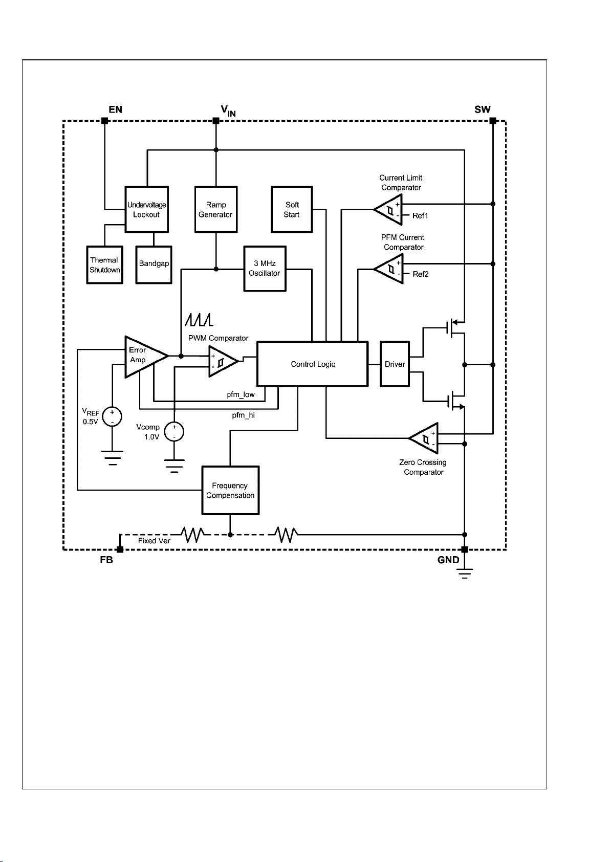
Block Diagram
30008418
FIGURE 3. Simplified Functional Diagram
5 www.national.com
LM3677
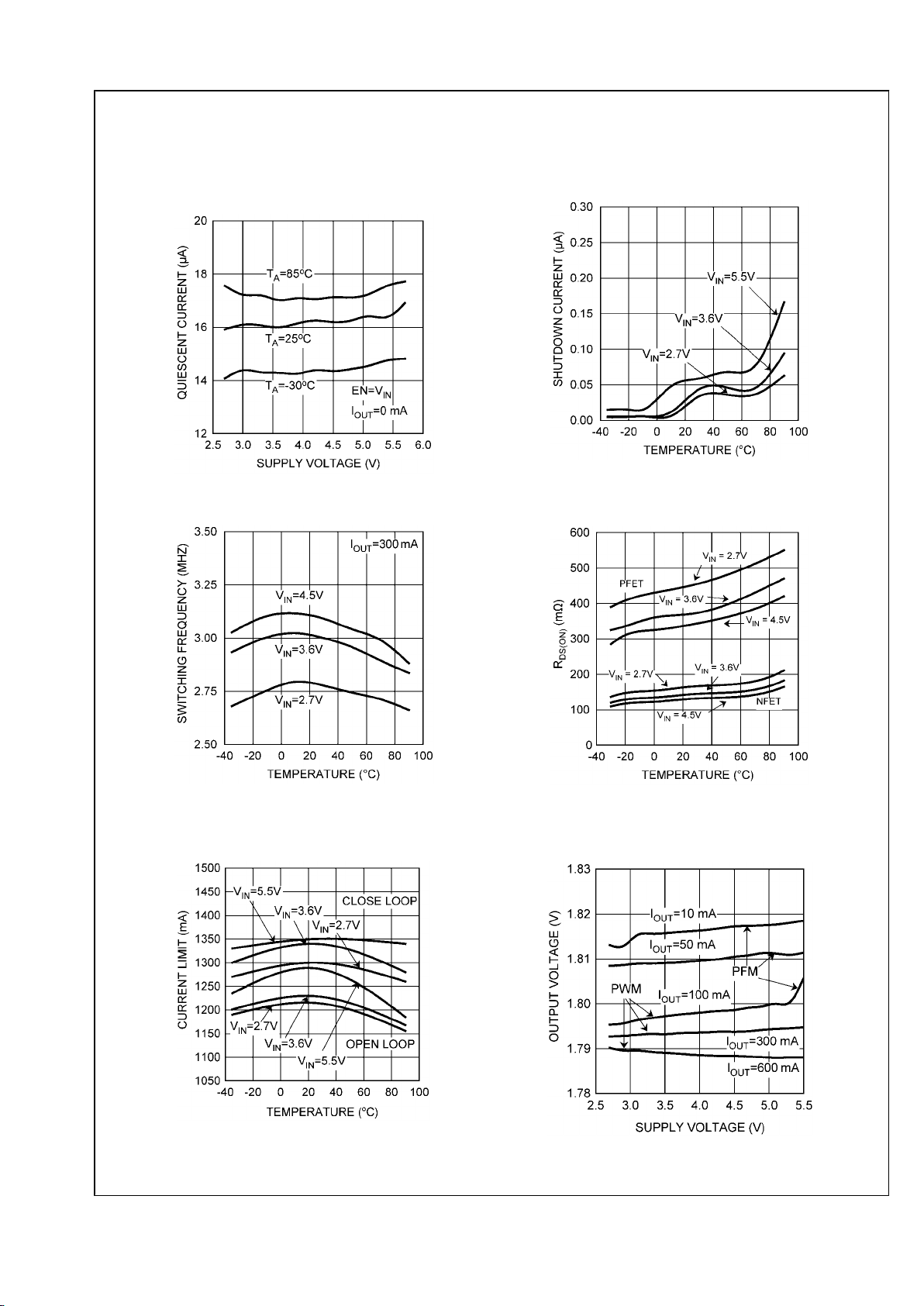
Typical Performance Characteristics
LM3677TL, Circuit of Figure 1, VIN = 3.6V, V
OUT
= 1.8V, TA = 25°C, unless otherwise noted.
Quiescent Supply Current vs. Supply Voltage
(Switching)
30008481
Shutdown Current vs. Temp
30008482
Switching Frequency vs. Temperature
30008483
R
DS(ON)
vs. Temperature
30008451
Open/Closed Loop Current Limit
vs. Temperature
30008449
Output Voltage vs. Supply Voltage
(V
OUT
= 1.8V)
30008484
www.national.com 6
LM3677
 Loading...