

NSC LM3668SD-3.3, LM3668 Datasheet
July 2007
LM3668
1A, High Efficiency Dual Mode Single Inductor Buck-Boost
DC/DC Converter
General Description
The LM3668 is a synchornous buck-boost DC-DC converter
optimized for powering low voltage circuits from a Li-Ion battery and input voltage rails between 2.5V and 5.5V. It has the
capability to support up to 1A output current over a output
voltage range of 2.8V/3.3V. The LM3668 regulates the output
voltage over the complete input voltage range by automatically switching between buck or boost modes depending on
the input voltage.
The LM3668 has 2 N-channel MOSFETS and 2 P-channel
MOSFETS arranged in a topology that provides continuous
operation through the buck and boost operating modes.
There is a MODE pin that allows the user to choose between
an intelligent automatic PFM-PWM mode operation and
forced PWM operation. During PWM mode, a fixed-frequency
2.2MHz (typ.) is used. PWM mode drives load up to 1A. Hysteretic PFM mode extends the battery life through reduction
of the quiescent current to 45µA (typ.) at light loads during
system standby. Internal synchronous rectification provides
high efficiency. In shutdown mode (Enable pin pulled low) the
device turns off and reduces battery consumption to 0.01µA
(typ.).
The LM3668 is available in a 12-pin LLP package. A high
switching frequency of 2.2MHz (typ.) allows the use of tiny
surface-mount components including a 2.2µH inductor, a
10µF input capacitor, and a 22µF output capacitor.
Features
■
45µA typical quiescent current
■
1A maximum load current for VIN = 2.8V to 5.5V
■
800mA maximum load current for VIN = 2.7V
■
600mA maximum load current for VIN = 2.5V
■
2.2 MHz PWM fixed switching frequency (typ.)
■
Automatic PFM-PWM Mode or Forced PWM Mode
■
Wide Input Voltage Range: 2.5V to 5.5V
■
Output Voltage Range: 2.8V/3.3V
■
Internal synchronous rectification for high efficiency
■
Internal soft start: 600µs Maximum start-up time
■
0.01µA typical shutdown current
■
Current overload and Thermal shutdown protection
■
Frequency Sync Pin: 1.6Mhz to 2.7MHz
Applications
■
Handset Peripherals
■
MP3 players
■
Pre-Regulation for linear regulators
■
PDAs
■
Portable Hard Disk Drives
■
WiMax Modems
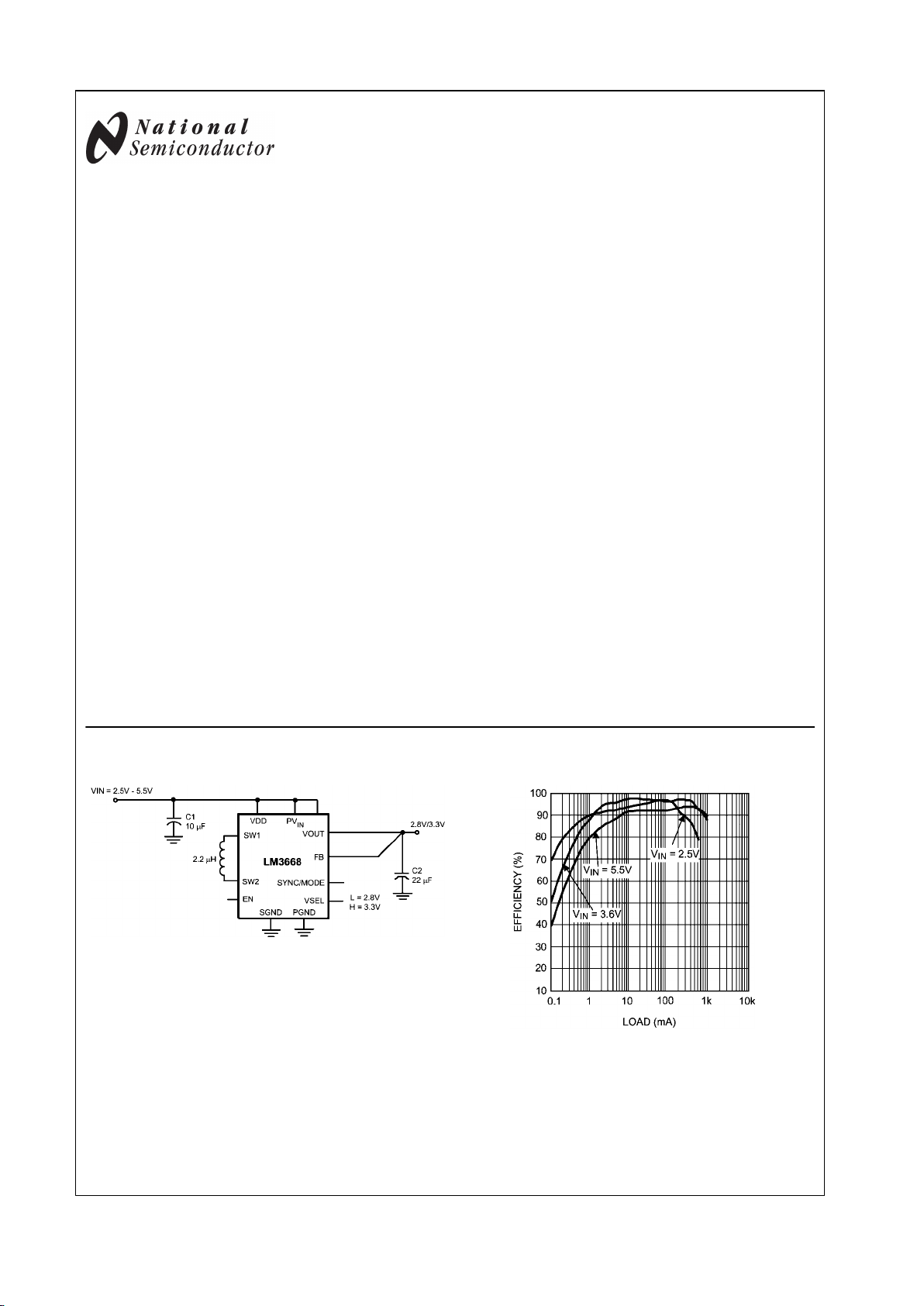
Typical Applications
20191401
Typical Application Circuit
20191425
Efficiency at 3.3V Output
© 2007 National Semiconductor Corporation 201914 www.national.com
LM3668 1A, High Efficiency Dual Mode Single Inductor Buck-Boost DC/DC Converter
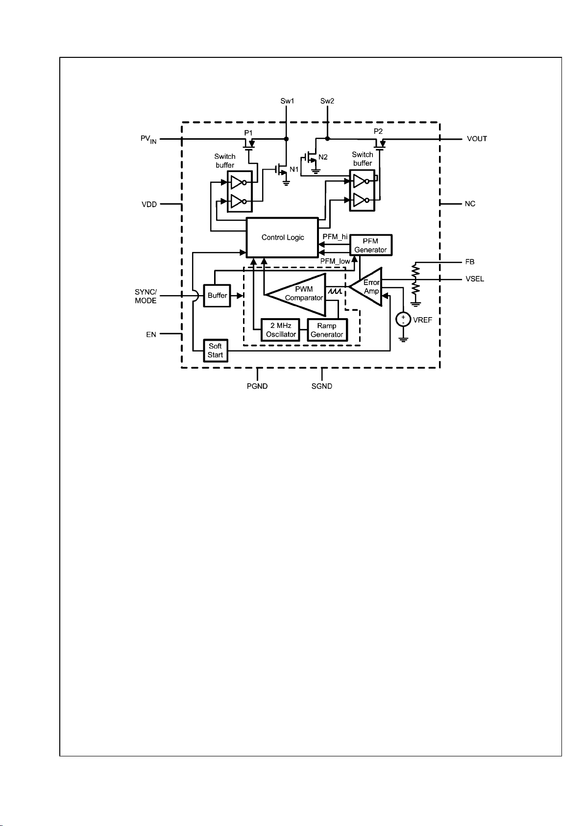
Functional Block Diagram
20191404
FIGURE 1. Functional Block Diagram
www.national.com 2
LM3668
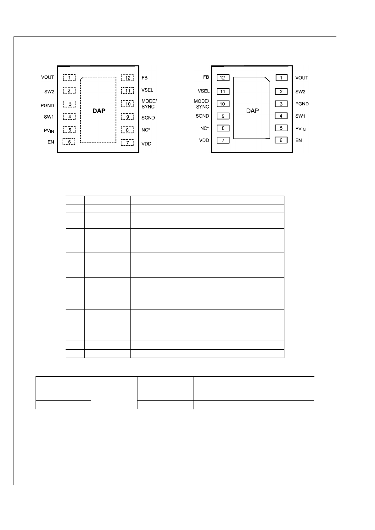
Connection Diagrams and Package Mark Information
20191402
Top View
20191403
Bottom View
Pin Descriptions
Pin # Pin Name Description
1 VOUT Connect to output capacitor.
2 SW2 Switching Node connection to the internal PFET switch (P2) and
NFET synchronous rectifier (N2).
3 PGND Power Ground.
4 SW1 Switching Node connection to the internal PFET switch (P1) and
NFET synchronous rectifier (N1).
5 PV
IN
Supply to the power switch, connect to the input capacitor.
6 EN Enable Input. Set this digital input high for normal operation. For
shutdown, set low.
7 VDD Signal Supply input. If board layout is not optimum an optional
1µF ceramic capacitor is suggested as close to this pin as
possible.
8 NC* No connect. Connect this pin to GND on PCB layout.
9 SGND Analog and Control Ground.
10 MODE/SYNC Mode = LOW, Automatic Mode. Mode= HI, Forced PWM Mode
SYNC = external clock synchronization from 1.6MHz to 2.7MHz
(When SYNC function is used, device is forced in PWM mode).
11 VSEL Logic input low = 2.8V and logic high = 3.3V to set output Voltage.
12 FB Feedback Analog Input. Connect to the output at the output filter.
Ordering Information
Order Number Package
NSC Package
Marking
Supplied As
LM3668SD - 3.3
LLP-12
S016B 1000 units, Tape and Reel
LM3668SDX - 3.3 S016B 4500 units, Tape and Reel
3 www.national.com
LM3668
Absolute Maximum Ratings (Note 1)
If Military/Aerospace specified devices are required,
please contact the National Semiconductor Sales Office/
Distributors for availability and specifications.
PV
IN, VDD
Pin, SW1, SW2 & V
OUT
:
Voltage to SGND & PGND
−0.2V to +6.0V
FB, EN,MODE,SYNC pin: (PGND &
SGND-0.2V) to
(PVIN + 0.2)
PGND to SGND -0.2V to 0.2V
Continuous Power Dissipation
(Note 3)
Internally Limited
Maximum Junction Temperature
(T
J-MAX
)
+125°C
Storage Temperature Range −65°C to +150°C
Maximum Lead Temperature
(Soldering, 10 sec)
+260°C
Operating Ratings
Input Voltage Range 2.5V to 5.5V
Recommended Load Current 0mA to 1A
Junction Temperature (TJ) Range −40°C to +125°C
Ambient Temperature (TA) Range
(Note 3)
−40°C to +85°C
Thermal Properties
Junction-to-Ambient Thermal Resistance (θJA),
34°C/W
Leadless Lead frame Package (Note 5)
Electrical Characteristics (Notes 6, 7) Limits in standard typeface are for T
J
= +25°C. Limits in boldface type
apply over the full operating ambient temperature range (−40°C ≤ = TA ≤ +85°C). Unless otherwise noted: specifications apply to
the LM3668. VIN = 3.6V = EN, V
OUT
= 3.3V, CIN = 10 µF & C
OUT
= 22µF (Note 8).
Symbol Parameter Conditions Min Typ Max Units
V
FB
Feedback Voltage (Note 7)
-3 3 %
I
LIM
Switch Peak Current Limit Open loop(Note 2)
1.6 1.85 2.05 A
I
SHDN
Shutdown Supply Current EN =0V
0.01
1
µA
I
Q_PFM
DC Bias Current in PFM No load, device is not switching
(FB Forced higher than
programmed output voltage)
45 60 µA
I
Q_PWM
DC Bias Current in PWM PWM Mode, No Switching
600 750 µA
R
DSON(P)
Pin-Pin Resistance for PFET Switches P1 and P2
130 180
mΩ
R
DSON(N)
Pin-Pin Resistance for NFET Switches N1 and N2
100 150
mΩ
F
OSC
Internal Oscillator Frequency PWM Mode
1.9 2.2 2.5 MHz
F
SYNC
Sync Frequency Range VIN = 3.6V
1.6 2.7 MHz
V
IH
Logic High Input for EN, MODE/
SYNC pins
1.1 V
V
IL
Logic Low Input for EN, MODES/
SYNC pins
0.4 V
I
EN, MODE, SYNC
EN,MODES/SYNC pin Input Current
0.3 1 µA
Note 1: Absolute Maximum Ratings indicate limits beyond which damage to the component may occur. Operating Ratings are conditions under which operation
of the device is guaranteed. Operating Ratings do not imply guaranteed performance limits. For guaranteed performance limits and associated test conditions,
see the Electrical Characteristics tables.
Note 2: Electrical Characteristic table reflects open loop data (FB = 0V and current drawn from SW pin ramped up until cycle by cycle current limits is activated).
Closed loop current limit is the peak inductor current measured in the application circuit by increasing output current until output voltage drops by 10%.
Note 3: In applications where high power dissipation and/or poor package thermal resistance is present, the maximum ambient temperature may have to be
derated. Maximum ambient temperature (T
A-MAX
) is dependent on the maximum operating junction temperature (T
J-MAX-OP
= 125ºC), the maximum power
dissipation of the device in the application (P
D-MAX
), and the junction-to ambient thermal resistance of the part/package in the application (θJA), as given by the
following equation: T
A-MAX
= T
J-MAX-OP
– (θJA × P
D-MAX
).
Note 4: The Human body model is a 100 pF capacitor discharged through a 1.5 kΩ resistor into each pin. The machine model is a 200 pF capacitor discharged
directly into each pin. MIL-STD-883 3015.7
Note 5: Junction-to-ambient thermal resistance (θJA) is taken from a thermal modeling result, performed under the conditions and guidelines set forth in the
JEDEC standard JESD51-7. The test board is a 4-layer FR-4 board measuring 101.6mm x 76.2mm x 1.6mm. Thickness of the copper layers are 2oz/1oz/1oz/
2oz. The middle layer of the board is 60mm x 60mm. Ambient temperature in simulation is 22°C, still air.
Junction-to-ambient thermal resistance is highly application and board-layout dependent. In applications where high maximum power dissipation exists, special
care must be paid to thermal dissipation issues in board design.
Note 6: All voltage is with respect to SGND.
Note 7: Min and Max limits are guaranteed by design, test, or statistical analysis. Typical numbers are not guaranteed, but do represent the most likely norm.
Note 8: CIN and C
OUT
: Low-ESR Surface-Mount Ceramic Capacitors (MLCCs) used in setting electrical characteristics.
www.national.com 4
LM3668
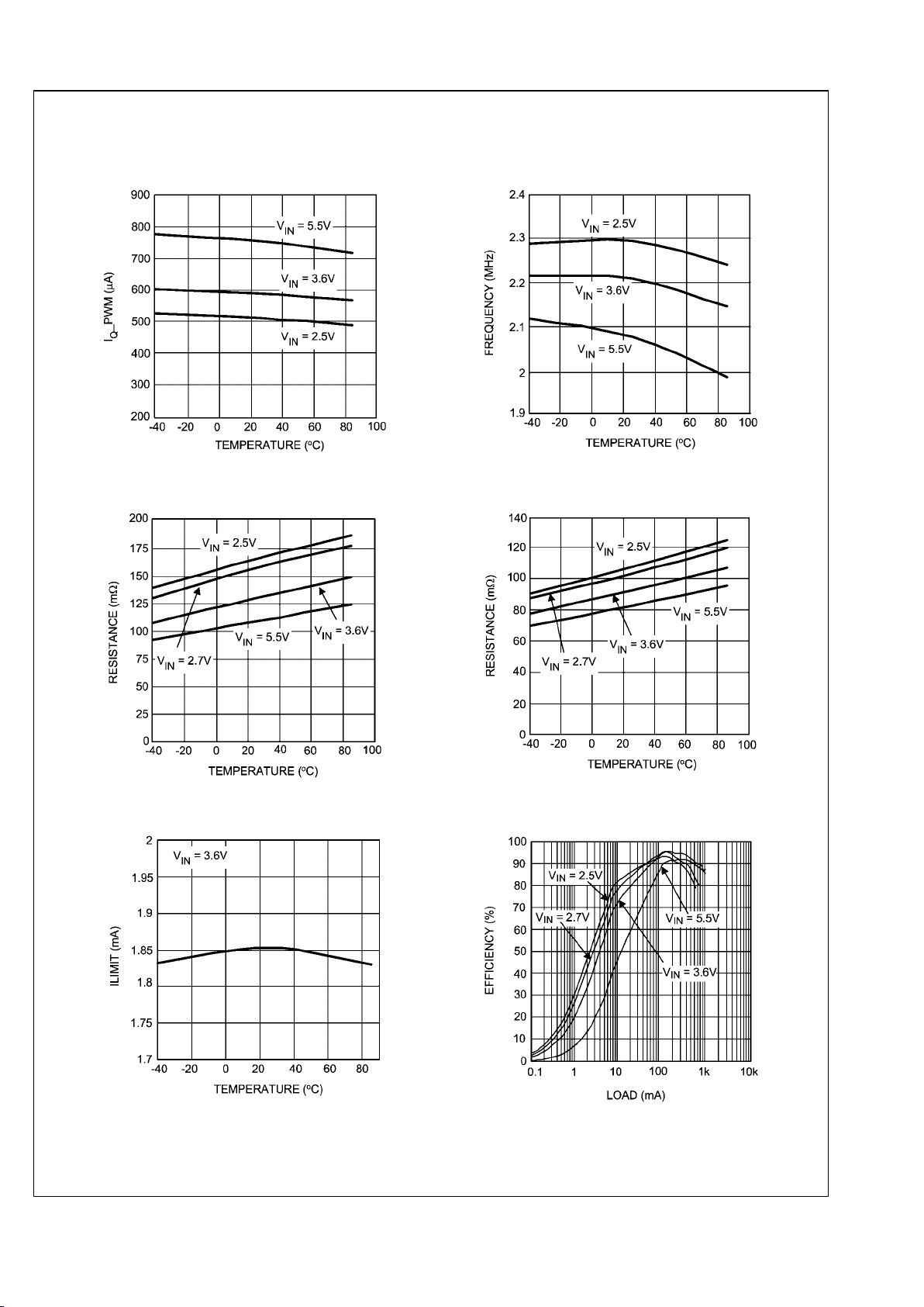
Typical Performance Characteristics Typical Application circuit Figure 1, V
IN
= 3.6V, L = 2.2µH, CIN =
10µF, C
OUT
= 22µF , TA = 25°C , Unless otherwise Stated.
Supply Current vs. Temperature ( Not switching)
20191439
Switching Frequency vs. Temperature
20191438
P_FET R
DS(ON)
vs. Temperature
20191442
N_FET R
DS(ON)
vs. Temperature
20191441
ILimit vs. Temperature
20191437
Efficiency at V
OUT
= 2.8V ( Forced PWM Mode)
20191427
5 www.national.com
LM3668
 Loading...