

NSC LM363H-100, LM363H-500, LM363H-10 Datasheet
LM363 Precision Instrumentation Amplifier
General Description
The LM363 is a monolithic true instrumentation amplifier. It
requires no external parts for fixed gains of 10, 100 and
1000. High precision is attained by on-chip trimming of offset voltage and gain. A super-beta bipolar input stage gives
very low input bias current and voltage noise, extremely low
offset voltage drift, and high common-mode rejection ratio.
A two-stage amplifier design yields an open loop gain of
10,000,000 and a gain bandwidth product of 30 MHz, yet
remains stable for all closed loop gains. The LM363 operates with supply voltages from
g
5V tog18V with only
1.5 mA current drain.
The LM363’s low voltage noise, low offset voltage and offset voltage drift make it ideal for amplifying low-level, lowimpedance transducers. At the same time, its low bias current and high input impedance (both common-mode and
differential) provide excellent performance at high impedance levels. These features, along with its ultra-high common-mode rejection, allow the LM363 to be used in the
most demanding instrumentation amplifier applications, replacing expensive hybrid, module or multi-chip designs. Because the LM363 is internally trimmed, precision external
resistors and their associated errors are eliminated.
The 16-pin dual-in-line package provides pin-strappable
gains of 10, 100 or 1000. Its twin differential shield drivers
eliminate bandwidth loss due to cable capacitance. Compensation pins allow overcompensation to reduce bandwidth and output noise, or to provide greater stability with
capacitive loads. Separate output force, sense and reference pins permit gains between 10 and 10,000 to be programmed using external resistors.
On the 8-pin metal can package, gain is internally set at 10,
100 or 500 but may be increased with external resistors.
The shield driver and offset adjust pins are omitted on the
8-pin versions.
The LM363 is rated for 0
Features
Y
Offset and gain pretrimmed
Y
12 nV/0Hz input noise (Ge500/1000)
Y
130 dB CMRR typical (Ge500/1000)
Y
2 nA bias current typical
Y
No external parts required
Y
Dual shield drivers
Y
Can be used as a high performance op amp
Y
Low supply current (1.5 mA typ)
Cto70§C.
§
LM363 Precision Instrumentation Amplifier
April 1991
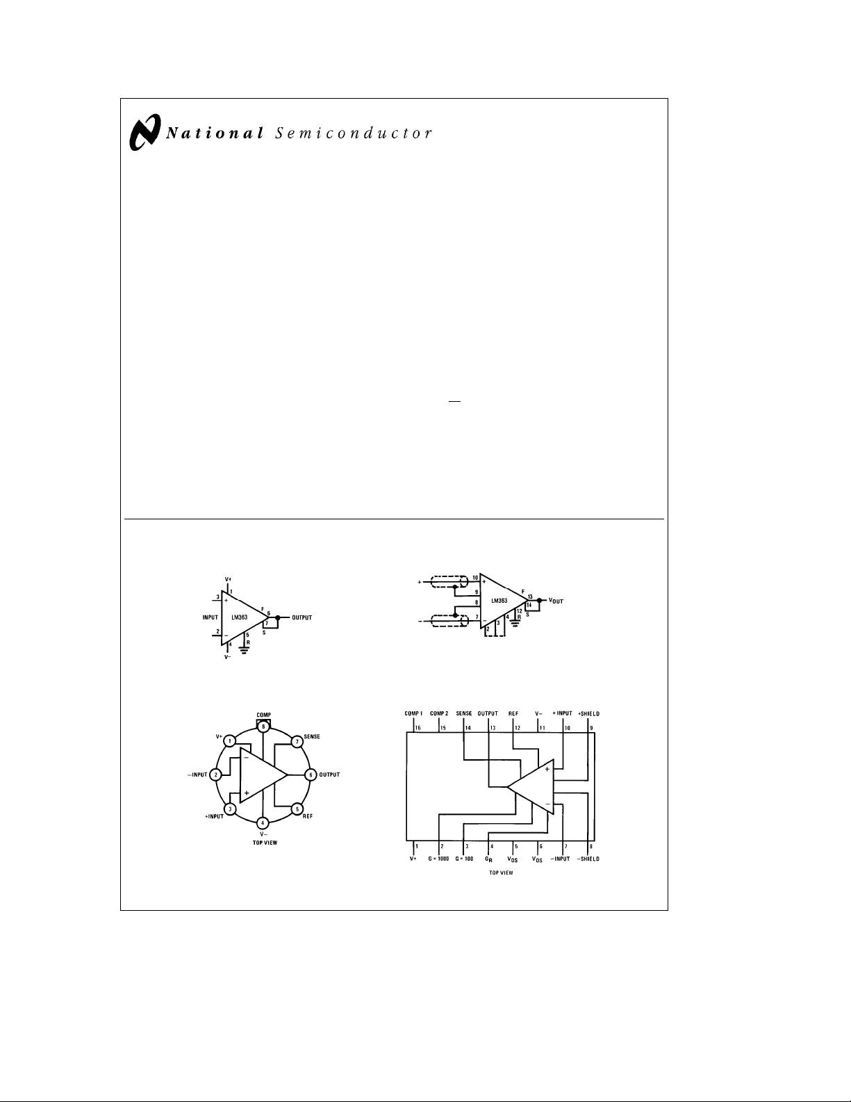
Typical Connections
8-Pin Package
TL/H/5609– 1
16-Pin Package
Ge10 2, 3, 4, open
e
100 3 –4 shorted
G
e
1000 2 –4 shorted
G
TL/H/5609– 33
Connection Diagrams
Metal Can Package 16-Pin Dual-In-Line Package
Order Number LM363H-10,
LM363H-100 or LM363H-500
See NS Package Number H08C
C
1995 National Semiconductor Corporation RRD-B30M115/Printed in U. S. A.
TL/H/5609
Order Number 363D
See NS Package Number D16C
TL/H/5609– 2
Absolute Maximum Ratings (Note 5)
If Military/Aerospace specified devices are required,
please contact the National Semiconductor Sales
Office/Distributors for availability and specifications.
g
g
18V
g
10V
20 mA
Supply Voltage
Differential Input Voltage
Input Current
Input Voltage Equal to Supply Voltage
Reference and Sense Voltage
Lead Temp. (Soldering, 10 sec.) 300§C
ESD rating to be determined.
LM363 Electrical Characteristics (Notes 1 and 2)
LM363
Parameter Conditions
Typ Limit Limit
FIXED GAIN (8-PIN)
Input Offset Voltage Ge500 30 150 400 mV
e
G
100 50 250 700 mV
e
G
10 0.5 2.5 6 mV
Input Offset Voltage Drift Ge500 1 4 mV/§C
e
G
100 2 8 mV/§C
e
G
10 20 75 mV/§C
Gain Error Ge500 0.1 0.8 0.9 %
g
(
10V Swing, 2 kX Load) Ge100 0.07 0.7 0.8 %
e
G
10 0.05 0.6 0.7 %
PROGRAMMABLE GAIN (16-PIN)
Input Offset Voltage Ge1000 50 250 500 mV
e
G
100 100 450 900 mV
e
G
10 1 3.5 8 mV
Input Offset Voltage Drift Ge1000 1 5 mV/§C
e
G
100 2 10 mV/§C
e
G
10 10 100 mV/§C
Gain Error Ge1000 2.0 3.0 3.5 %
g
(
10V Swing, 2 kX Load) Ge100 0.1 0.7 0.8 %
e
G
10 0.6 2.0 2.3 %
FIXED GAIN AND PROGRAMMABLE
Gain Temperature Coefficient Ge1000 40 ppm/§C
e
G
500 20 ppm/§C
e
G
100, 10 10 ppm/§C
Gain Non-Linearity Ge10, 100 0.01 0.03 0.04 %
g
(
10V Swing, 2 kX Load) Ge500, 1000 0.01 0.05 0.06 %
Tested Design
(Note 3) (Note 4)
g
Units
25V
2
LM363 Electrical Characteristics (Continued) (Notes 1 and 2)
LM363
Parameter Conditions
Typ Limit Limit
Common-Mode Rejection Ge1000, 500 130 114 104 dB
Ratio (
b
10VsV
s
10V) Ge100 120 94 84 dB
CM
Ge10 105 90 80 dB
Positive Supply Rejection Ge1000, 500 130 110 100 dB
Ratio (5V to 15V) G
e
100 120 100 95 dB
e
G
10 100 85 78 dB
Negative Supply Rejection Ge1000, 500 120 100 90 dB
b
Ratio (
5V tob15V) Ge100 106 85 75 dB
e
G
10 86 70 60 dB
Input Bias Current 2 10 20 nA
Input Offset Current 1 3 5 nA
Common-Mode Input 100 8 GX
Resistance
Differential Mode Input Ge1000, 500 0.2 GX
Resistance G
e
100 2 GX
Ge10 20 GX
Input Offset Current Change
b
11VsV
s
13V 20 100 300 pa/V
CM
Reference and Sense 50 kX
Resistance Min 30 27 kX
Max 80 83 kX
Open Loop Gain G
e
1000, 500 10 1 V/mV
CL
Supply Current Positive 1.2 2.4 3.0 mA
Negative 1.6 2.8 3.4 mA
a
b
e
eb
Note 1: These conditions apply unless otherwise noted; V
e
25§C.
T
j
Note 2: Boldface limits are guaranteed over full temperature range. Operating ambient temperature range is 0
Note 3: Guaranteed and 100% production tested.
Note 4: Guaranteed but not 100% tested. These limits are not used in determining outgoing quality levels.
Note 5: Maximum rated junction temperature is 100
for the ceramic DIP (D).
15V, V
C for the LM363. Thermal resistance, junction to ambient, is 150§C/W for the TO-99(H) package and 100§C/W
§
15V, V
e
0V, R
CM
L
Tested Design
(Note 3) (Note 4)
e
2kX, reference pin grounded, sense pin connected to output and
Cto70§C for the LM363.
§
Units
3
Typical Performance Characteristics T
Parameter
e
25§C
A
Fixed Gain and Programmable
1000/500 100 10
Input Voltage Noise, rms, 1 kHz 12 18 90 nV/SHz
Input Voltage Noise (Note 6) 0.4 1.5 10 mVp-p
Input Current Noise, rms, 1 kHz 0.2 0.2 0.2 pA/SHz
Input Current Noise (Note 6) 40 40 40 pAp-p
Bandwidth 30 100 200 kHz
Slew Rate 1 0.36 0.24 V/ms
Settling Time, 0.1% of 10V 70 25 20 ms
Offset Voltage Warm-Up Drift (Note 7) 5 15 50 mV
Offset Voltage Stability (Note 8) 5 10 100 mV
Gain Stability (Note 8) 0.01 0.005 0.05 %
Note 6: Measured for 100 seconds in a 0.01 Hz to 10 Hz bandwidth.
Note 7: Measured for 5 minutes in still air, V
a
b
e
eb
15V, V
15V. Warm-up drift is proportionally reduced at lower supply voltages.
Units
Common-Mode Input
Voltage Limit
Output Swing Referred to
Supplies
Supply Current vs Supply
Voltage
Supply Current vs
Temperature
Input Bias Current vs
Temperature
Input Offset Current vs
Temperature
TL/H/5609– 3
4
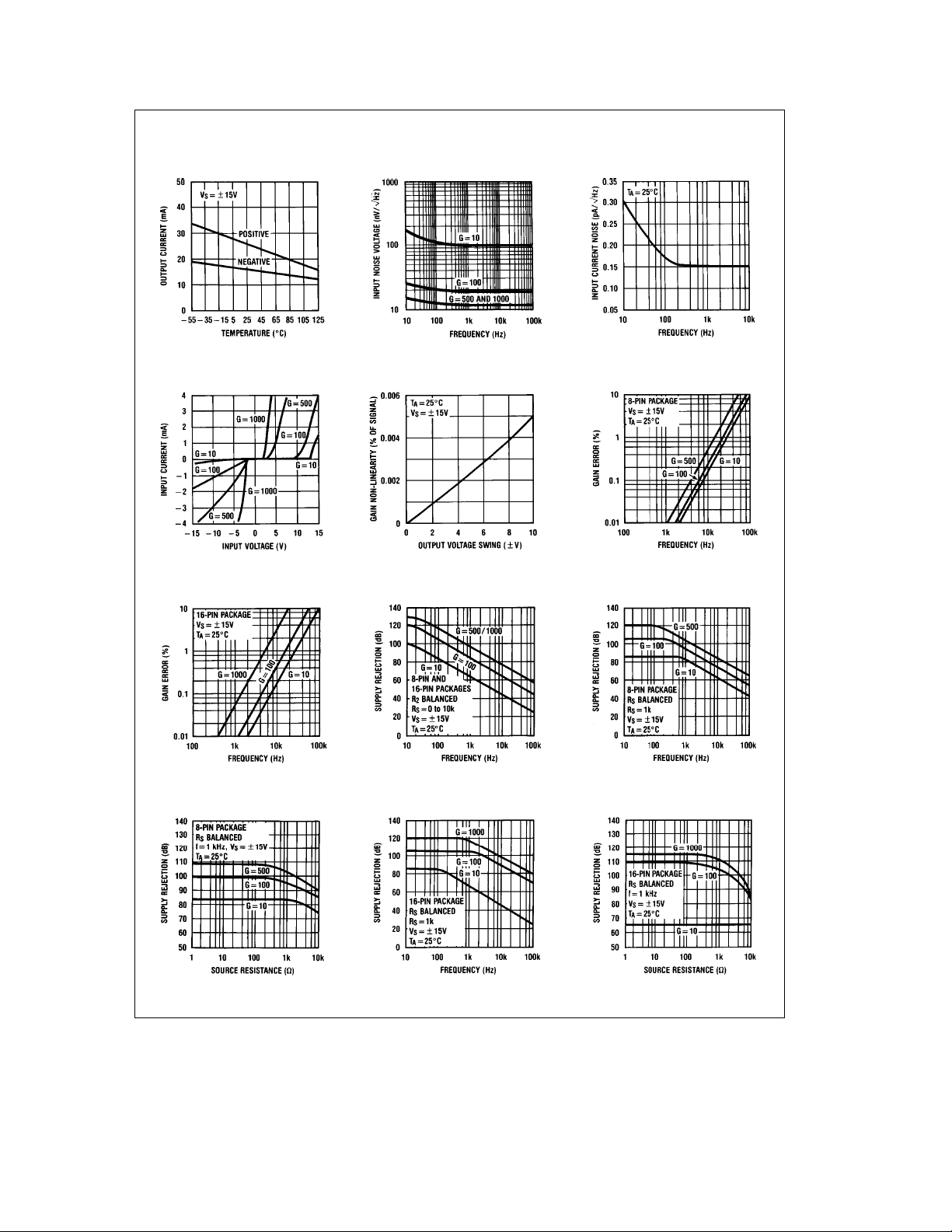
Typical Performance Characteristics (Continued)
Output Current Limit Input Noise Voltage Input Current Noise
Input Current vs Voltage
Overdrive Gain Non-Linearity Gain Error vs Frequency*
*Trimmed to zero at 100 Hz
Gain Error vs Frequency* Rejection Rejection
Positive Power Supply Negative Power Supply
*Trimmed to zero at 100 Hz
Negative Power Supply Negative Power Supply Negative Power Supply
Rejection Rejection Rejection
5
TL/H/5609– 4
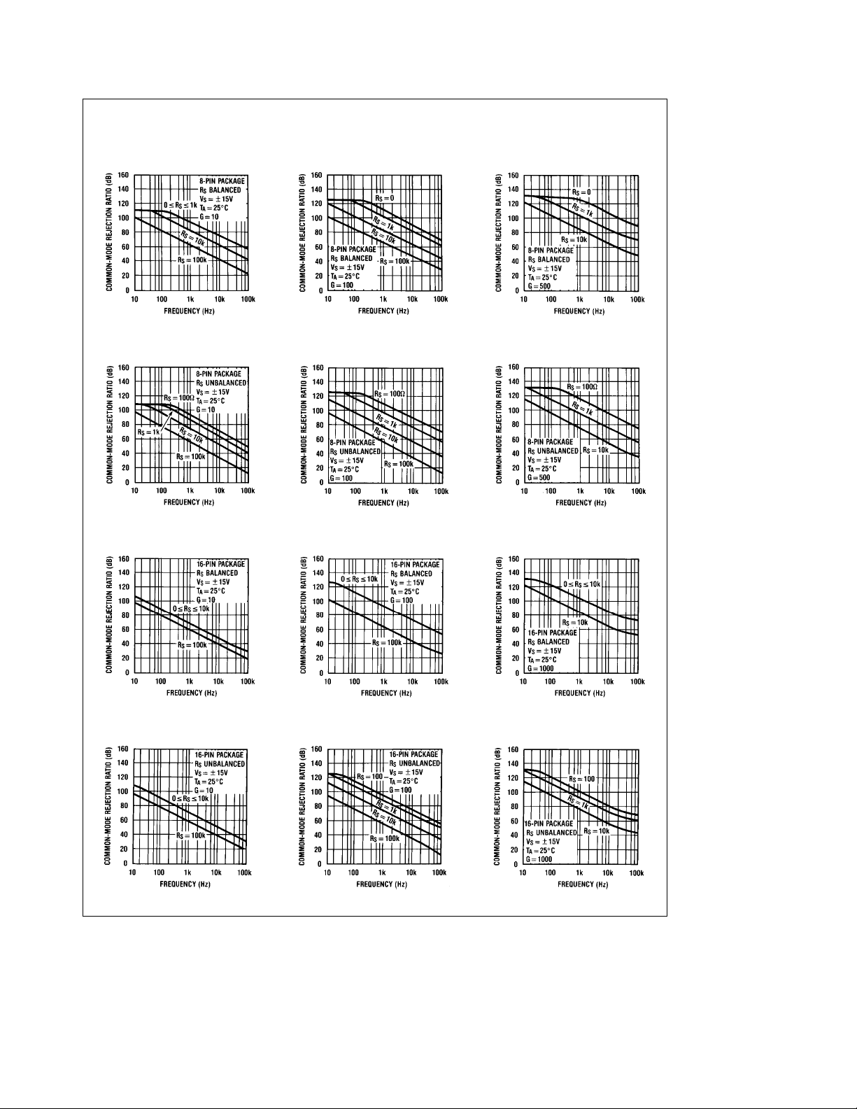
Typical Performance Characteristics (Continued)
CMRR with Balanced CMRR with Balanced CMRR with Balanced
Source Resistance Source Resistance Source Resistance
CMRR with Unbalanced CMRR with Unbalanced CMRR with Unbalanced
Source Resistance Source Resistance Source Resistance
CMRR with Balanced CMRR with Balanced CMRR with Balanced
Source Resistance Source Resistance Source Resistance
CMRR with Unbalanced CMRR with Unbalanced CMRR with Unbalanced
Source Resistance Source Resistance Source Resistance
TL/H/5609– 5
6
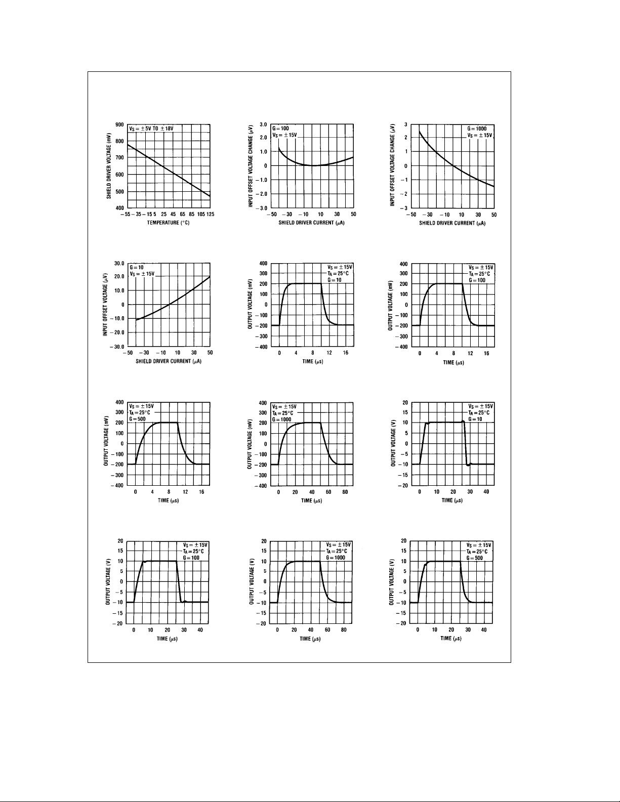
Typical Performance Characteristics (Continued)
Shield Driver Bias Voltage Shield Driver Loading Error Shield Driver Loading Error
Shield Driver Loading Error Response
Small Signal Transient
Response
Large Signal Transient
Response
Small Signal Transient
Small Signal Transient
Response
Large Signal Transient
Response
Small Signal Transient
Response
Large Signal Transient
Response
Large Signal Transient
Response
TL/H/5609– 6
7
 Loading...