

NSC LM361N, LM361MX, LM361MWC, LM361M Datasheet
LM161/LM261/LM361
High Speed Differential Comparators
General Description
The LM161/LM261/LM361 is a very high speed differential
input, complementary TTL output voltage comparator with
improved characteristics over the SE529/NE529 for which it
is a pin-for-pin replacement. The device has been optimized
for greater speed performance and lower input offset voltage. Typically delay varies only 3 ns for over-drive variations
of 5 mV to 500 mV. It may be operated fromopamp supplies
(
±
15V).
Complementary outputs having maximum skew are provided. Applications involve high speed analog to digital converters and zero-crossing detectors in disk file systems.
Features
n Independent strobes
n Guaranteed high speed: 20 ns max
n Tight delay matching on both outputs
n Complementary TTL outputs
n Operates from op amp supplies:
±
15V
n Low speed variation with overdrive variation
n Low input offset voltage
n Versatile supply voltage range
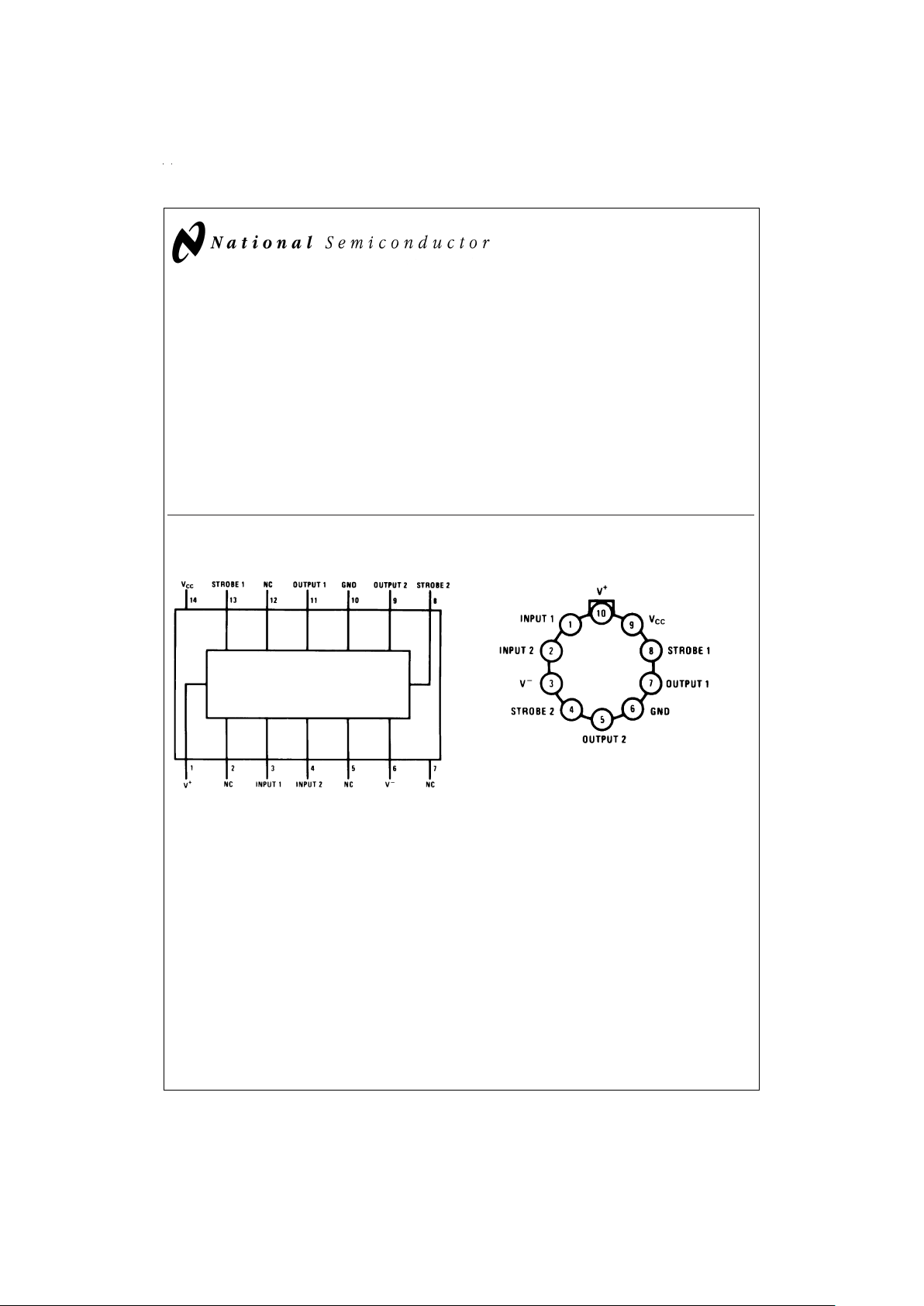
Connection Diagrams
Dual-In-Line Package
DS005708-2
Top View
Order Number LM161J
LM361M or LM361N
See NS Package Number M14A or N14A
Metal Can Package
DS005708-3
Order Number LM161H/883 (Note 1), or LM361H
See NS Package Number H10C
Note 1: Also available per SMD#5962-8757203
May 1999
LM161/LM261/LM361 High Speed Differential Comparators
© 1999 National Semiconductor Corporation DS005708 www.national.com
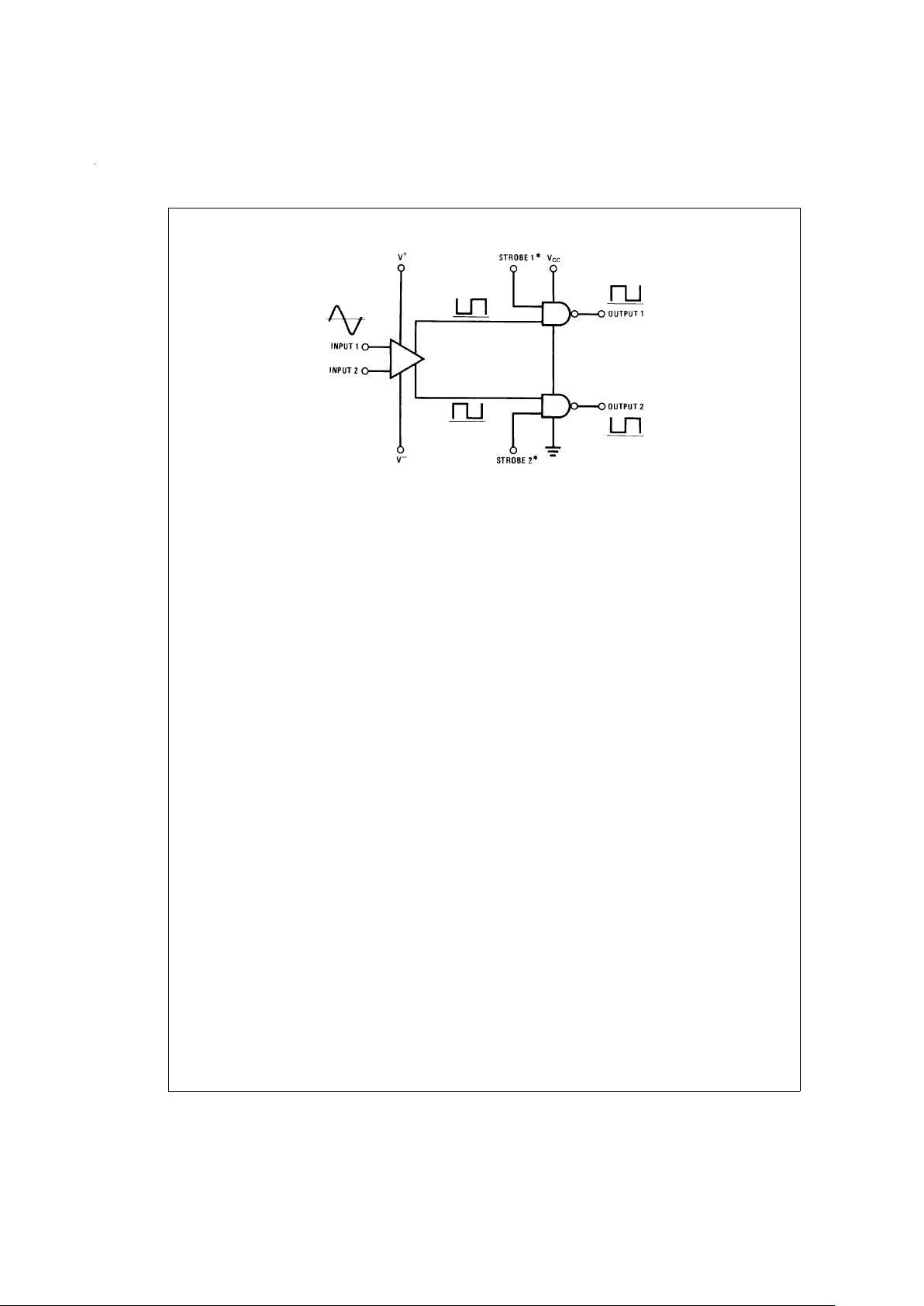
Logic Diagram
DS005708-4
*
Output is low when current is drawn from strobe pin.
www.national.com 2
Absolute Maximum Ratings (Note 2)
If Military/Aerospace specified devices are required,
please contact the National Semiconductor Sales Office/
Distributors for availability and specifications.
Positive Supply Voltage, V
+
+16V
Negative Supply Voltage, V
−
−16V
Gate Supply Voltage, V
CC
+7V
Output Voltage +7V
Differential Input Voltage
±
5V
Input Common Mode Voltage
±
6V
Power Dissipation 600 mW
Storage Temperature Range −65˚C to +150˚C
Operating Temperature Range T
MINTMAX
LM161 −55˚C to +125˚C
LM261 −25˚C to +85˚C
LM361 0˚C to +70˚C
Lead Temp. (Soldering, 10 seconds) 260˚C
For Any Device Lead Below V
−
0.3V
Operating Conditions
Min Typ Max
Supply Voltage V
+
LM161/LM261 5V 15V
LM361 5V 15V
Supply Voltage V
−
LM161/LM261 −6V −15V
LM361 −6V −15V
Supply Voltage V
CC
LM161/LM261 4.5V 5V 5.5V
LM361 4.75V 5V 5.25V
ESD Tolerance (Note 6) 1600V
Soldering Information
Dual-In-Line Package
Soldering (10 seconds) 260˚C
Small Outline Package
Vapor Phase (60 seconds) 215˚C
Infrared (15 seconds) 220˚C
See AN-450 “Surface Mounting Methods and Their Effect on
Product Reliability” for other methods of soldering surface
mount devices.
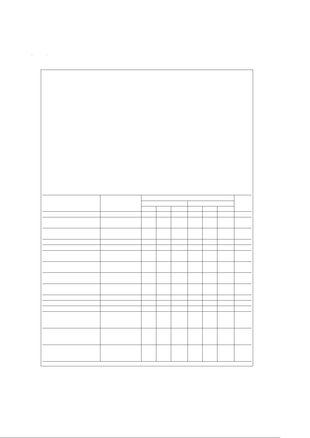
Electrical Characteristics
(V
+
=
+10V, V
CC
=
+5V, V
−
=
−10V, T
MIN
≤ TA≤ T
MAX
, unless noted)
Limits
Parameter Conditions LM161/LM261 LM361 Units
Min Typ Max Min Typ Max
Input Offset Voltage 1 3 1 5 mV
Input Bias Current T
A
=
25˚C 5 10 µA
20 30 µA
Input Offset Current T
A
=
25˚C 2 2 µA
35µA
Voltage Gain T
A
=
25˚C 3 3 V/mV
Input Resistance T
A
=
25˚C, f=1 kHz 20 20 kΩ
Logical “1” Output Voltage V
CC
=
4.75V, 2.4 3.3 2.4 3.3 V
I
SOURCE
=
−0.5 mA
Logical “0” Output Voltage V
CC
=
4.75V, 0.4 0.4 V
I
SINK
=
6.4 mA
Strobe Input “1” Current V
CC
=
5.25V, 200 200 µA
(Output Enabled) V
STROBE
=
2.4V
Strobe Input “0” Current V
CC
=
5.25V, −1.6 −1.6 mA
(Output Disabled) V
STROBE
=
0.4V
Strobe Input “0” Voltage V
CC
=
4.75V 0.8 0.8 V
Strobe Input “1” Voltage V
CC
=
4.75V 2 2 V
Output Short Circuit Current V
CC
=
5.25V, V
OUT
=
0V −18 −55 −18 −55 mA
V
+
=
10V, V
−
=
−10V,
V
CC
=
5.25V,
−55˚C≤T
A
≤125˚C
Supply Current I
+
4.5 mA
V
+
=
10V, V
−
=
−10V,
V
CC
=
5.25V,
0˚C≤T
A
≤70˚C
Supply Current I
+
5mA
V
+
=
10V, V
−
=
−10V,
V
CC
=
5.25V,
−55˚C≤T
A
≤125˚C
Supply Current I
−
10 mA
www.national.com3
 Loading...