

LM359
Dual, High Speed, Programmable, Current Mode (Norton)
Amplifiers
General Description
The LM359 consists of two current differencing (Norton) input amplifiers. Design emphasis has been placed on obtaining high frequency performance and providing user programmable amplifier operating characteristics. Each amplifier is
broadbanded to provide a high gain bandwidth product, fast
slew rate and stable operation for an inverting closed loop
gain of 10 or greater. Pins for additional external frequency
compensation are provided. The amplifiers are designed to
operate from a single supply and can accommodate input
common-mode voltages greater than the supply.
Applications
n General purpose video amplifiers
n High frequency, high Q active filters
n Photo-diode amplifiers
n Wide frequency range waveform generation circuits
n All LM3900 AC applications work to much higher
frequencies
Features
n User programmable gain bandwidth product, slew rate,
input bias current, output stage biasing current and total
device power dissipation
n High gain bandwidth product (I
SET
=
0.5 mA)
400 MHz for A
V
=
10 to 100
30 MHz for A
V
=
1
n High slew rate (I
SET
=
0.5 mA)
60 V/µs for A
V
=
10 to 100
30 V/µs for A
V
=
1
n Current differencing inputs allow high common-mode
input voltages
n Operates from a single 5V to 22V supply
n Large inverting amplifier output swing, 2 mV to V
CC
−
2V
n Low spot noise,
for f>1 kHz
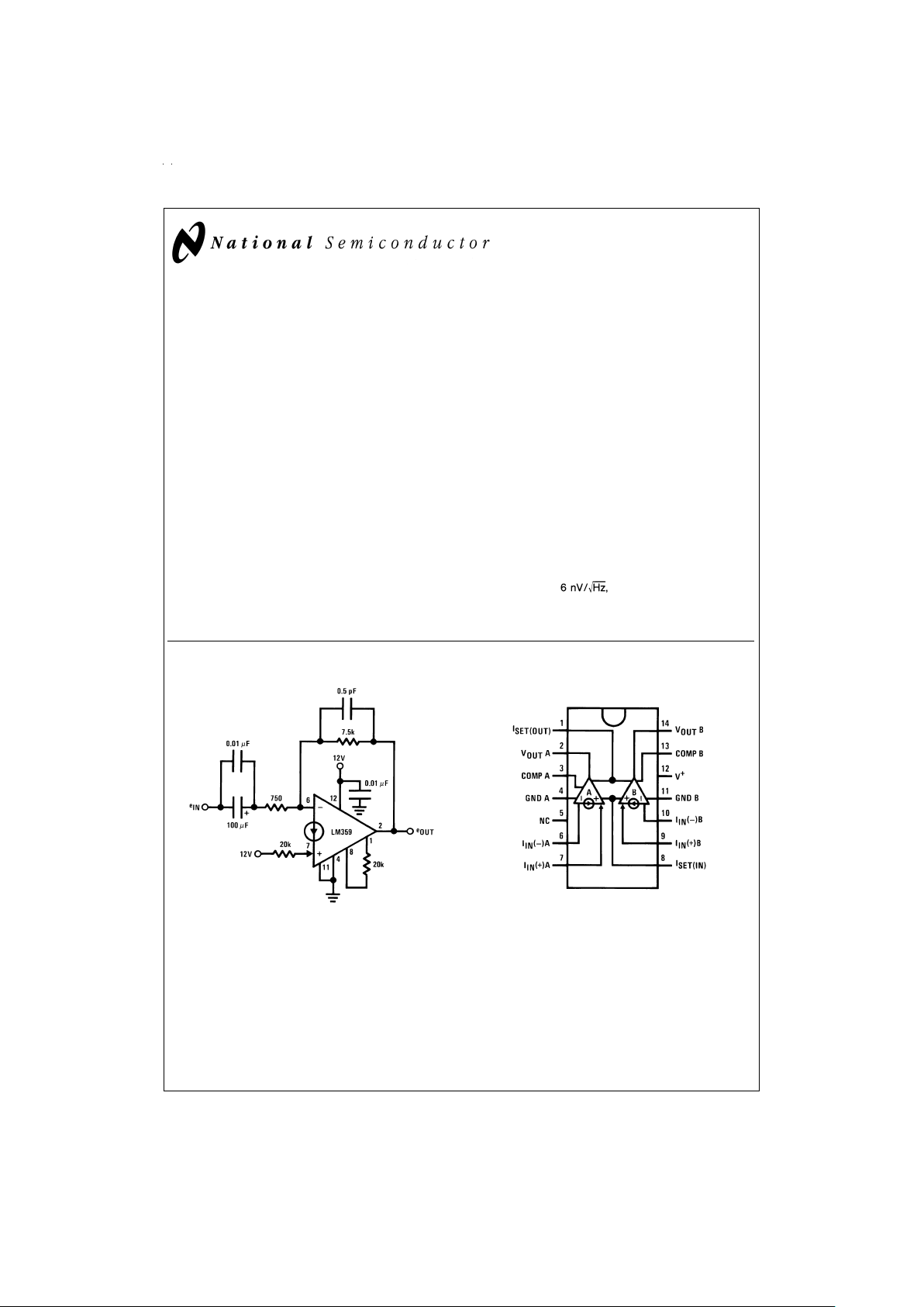
Typical Application Connection Diagram
DS007788-1
•
A
V
=
20 dB
•
−3 dB bandwidth=2.5 Hz to 25 MHz
•
Differential phase error<1˚ at 3.58 MHz
•
Differential gain error<0.5%at 3.58 MHz
Dual-In-Line Package
DS007788-2
Top View
Order Number LM359J, LM359M or LM359N
See NS Package Number J14A, M14A or N14A
October 1998
LM359 Dual, High Speed, Programmable, Current Mode (Norton) Amplifiers
© 1999 National Semiconductor Corporation DS007788 www.national.com
Absolute Maximum Ratings (Note 1)
If Military/Aerospace specified devices are required,
please contact the National Semiconductor Sales Office/
Distributors for availability and specifications.
Supply Voltage 22 V
DC
or±11 V
DC
Power Dissipation (Note 2)
J Package 1W
N Package 750 mW
Maximum T
J
J Package +150˚C
N Package +125˚C
Thermal Resistance
J Package
θ
jA
147˚C/W still air
110˚C/W with 400 linear feet/min air flow
N Package
θ
jA
100˚C/W still air
75˚C/W with 400 linear feet/min air flow
Input Currents, I
IN
(+) or IIN(−) 10 mA
DC
Set Currents, I
SET(IN)
or I
SET(OUT)
2mA
DC
Operating Temperature Range
LM359 0˚C to +70˚C
Storage Temperature Range −65˚C to +150˚C
Lead Temperature
(Soldering, 10 sec.) 260˚C
Soldering Information
Dual-In-Line Package
Soldering (10 sec.) 260˚C
Small Outline Package
Vapor Phase (60 sec.) 215˚C
Infrared (15 sec.) 220˚C
See AN-450 “Surface Mounting Methods and Their Effect
on Product Reliability” for other methods of soldering
surface mount devices.
ESD rating to be determined.
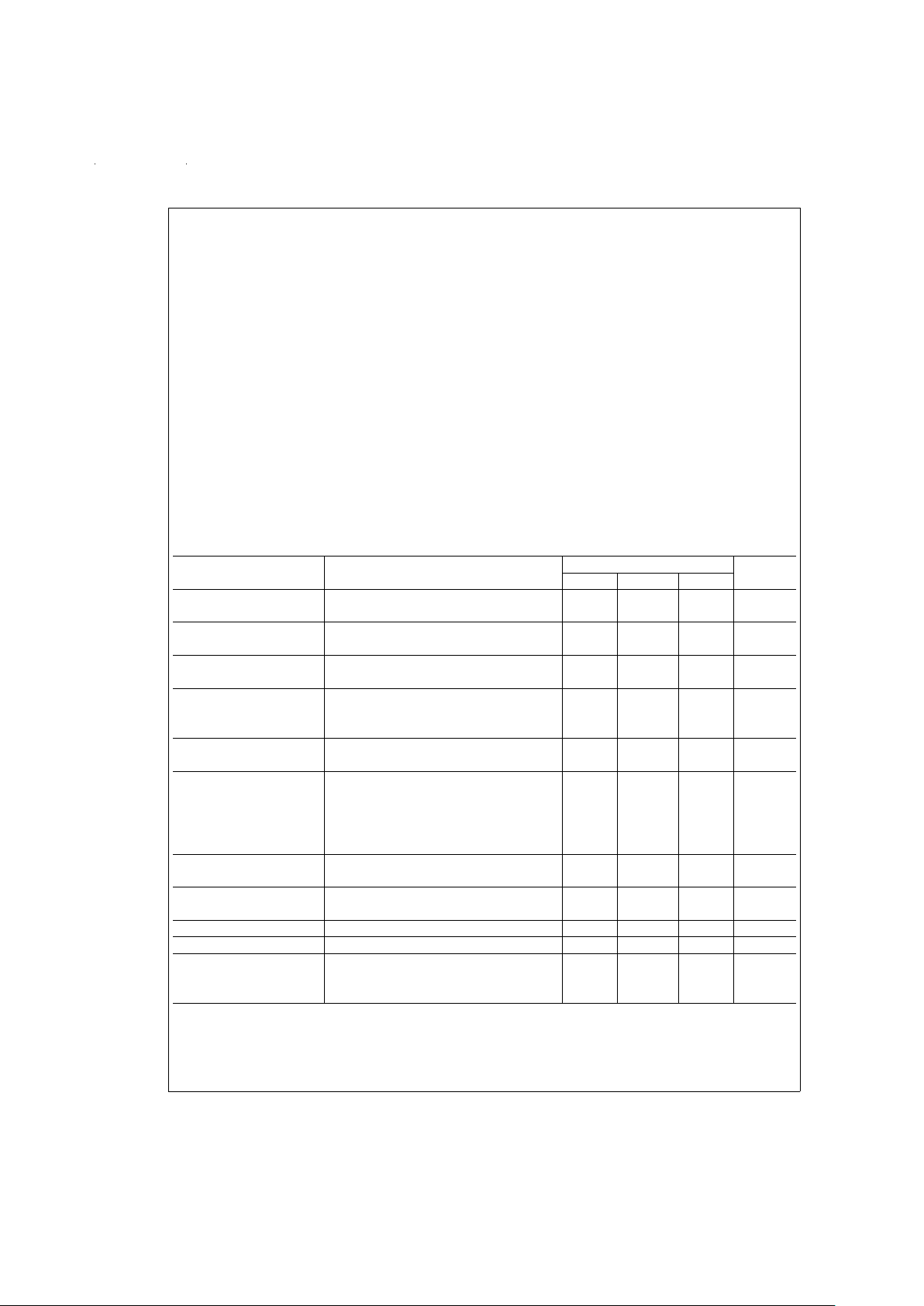
Electrical Characteristics
I
SET(IN)
=
I
SET(OUT)
=
0.5 mA, V
supply
=
12V, T
A
=
25˚C unless otherwise noted
Parameter Conditions LM359 Units
Min Typ Max
Open Loop Voltage V
supply
=
12V, R
L
=
1k, f=100 Hz 62 72 dB
Gain T
A
=
125˚C 68 dB
Bandwidth R
IN
=
1kΩ,C
comp
=
10 pF 15 30 MHz
Unity Gain
Gain Bandwidth Product R
IN
=
50Ω to 200Ω 200 400 MHz
Gain of 10 to 100
Slew Rate
Unity Gain R
IN
=
1kΩ,C
comp
=
10 pF 30 V/µs
Gain of 10 to 100 R
IN
<
200Ω 60 V/µs
Amplifier to Amplifier f=100 Hz to 100 kHz, R
L
=
1k −80 dB
Coupling
Mirror Gain at 2 mA I
IN
(+), I
SET
=
5 µA, T
A
=
25˚C 0.9 1.0 1.1 µA/µA
(Note 3) at 0.2 mA I
IN
(+), I
SET
=
5 µA 0.9 1.0 1.1 µA/µA
Over Temp.
at 20 µA I
IN
(+), I
SET
=
5 µA 0.9 1.0 1.1 µA/µA
Over Temp.
∆Mirror Gain at 20 µA to 0.2 mA I
IN
(+) 3 5
%
(Note 3) Over Temp, I
SET
=
5µA
Input Bias Current Inverting Input, T
A
=
25˚C 8 15 µA
Over Temp. 30 µA
Input Resistance (βre) Inverting Input 2.5 kΩ
Output Resistance I
OUT
=
15 mA rms, f=1 MHz 3.5 Ω
Output Voltage Swing R
L
=
600Ω
V
OUT
High IIN(−) and IIN(+) Grounded 9.5 10.3 V
V
OUT
Low IIN(−)=100 µA, IIN(+)=0 2 50 mV
www.national.com 2
Electrical Characteristics (Continued)
I
SET(IN)
=
I
SET(OUT)
=
0.5 mA, V
supply
=
12V, T
A
=
25˚C unless otherwise noted
Parameter Conditions LM359 Units
Min Typ Max
Output Currents
Source I
IN
(−) and IIN(+) Grounded, R
L
=
100Ω 16 40 mA
Sink (Linear Region) V
comp
−0.5V=V
OUT
=
1V, I
IN
(+)=0 4.7 mA
Sink (Overdriven) I
IN
(−)=100 µA, IIN(+)=0, 1.5 3 mA
V
OUT
Force=1V
Supply Current Non-Inverting Input 18.5 22 mA
Grounded, R
L
=
∞
Power Supply Rejection f=120 Hz, IIN(+) Grounded 40 50 dB
(Note 4)
Note 1: “Absolute Maximum Ratings” indicate limits beyond which damage to the device may occur. Operating Ratings indicate conditions for which the device is
functional, but do not guarantee specific performance limits.
Note 2: See Maximum Power Dissipation graph.
Note 3: Mirror gain is the current gain of the current mirror which is used as the non-inverting input.
∆Mirror Gain is the%change in AIfor two different mirror currents at any given temperature.
Note 4: See Supply Rejection graphs.
www.national.com3
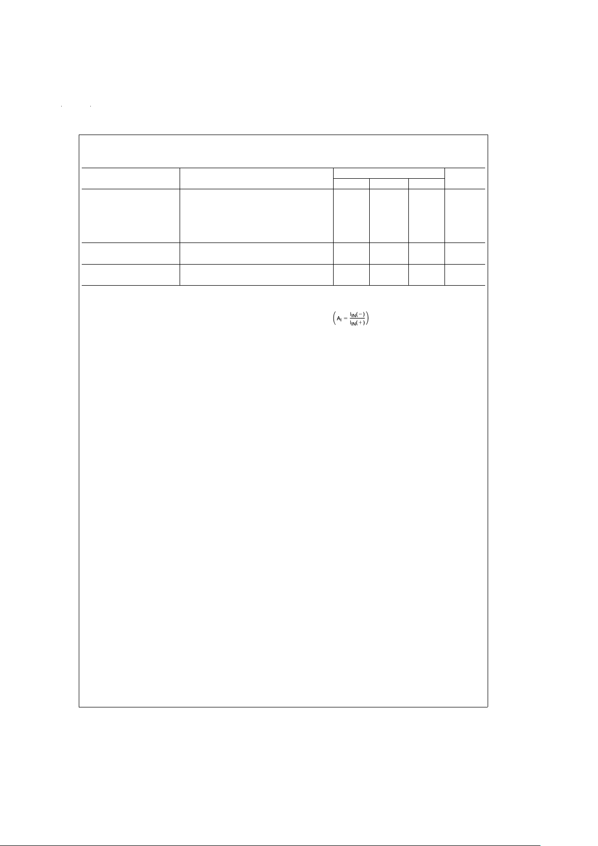
Schematic Diagram
DS007788-3
www.national.com 4
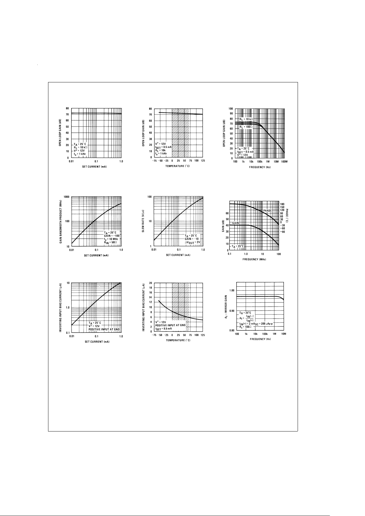
Typical Performance Characteristics
Open Loop Gain
DS007788-39
Open Loop Gain
DS007788-40
Note: Shaded area refers to LM359
Open Loop Gain
DS007788-41
Gain Bandwidth Product
DS007788-42
Slew Rate
DS007788-43
Gain and Phase
Feedback Gain=− 100
DS007788-44
Inverting Input Bias Current
DS007788-45
Inverting Input Bias Current
DS007788-46
Note: Shaded area refers to LM359
Mirror Gain
DS007788-47
www.national.com5
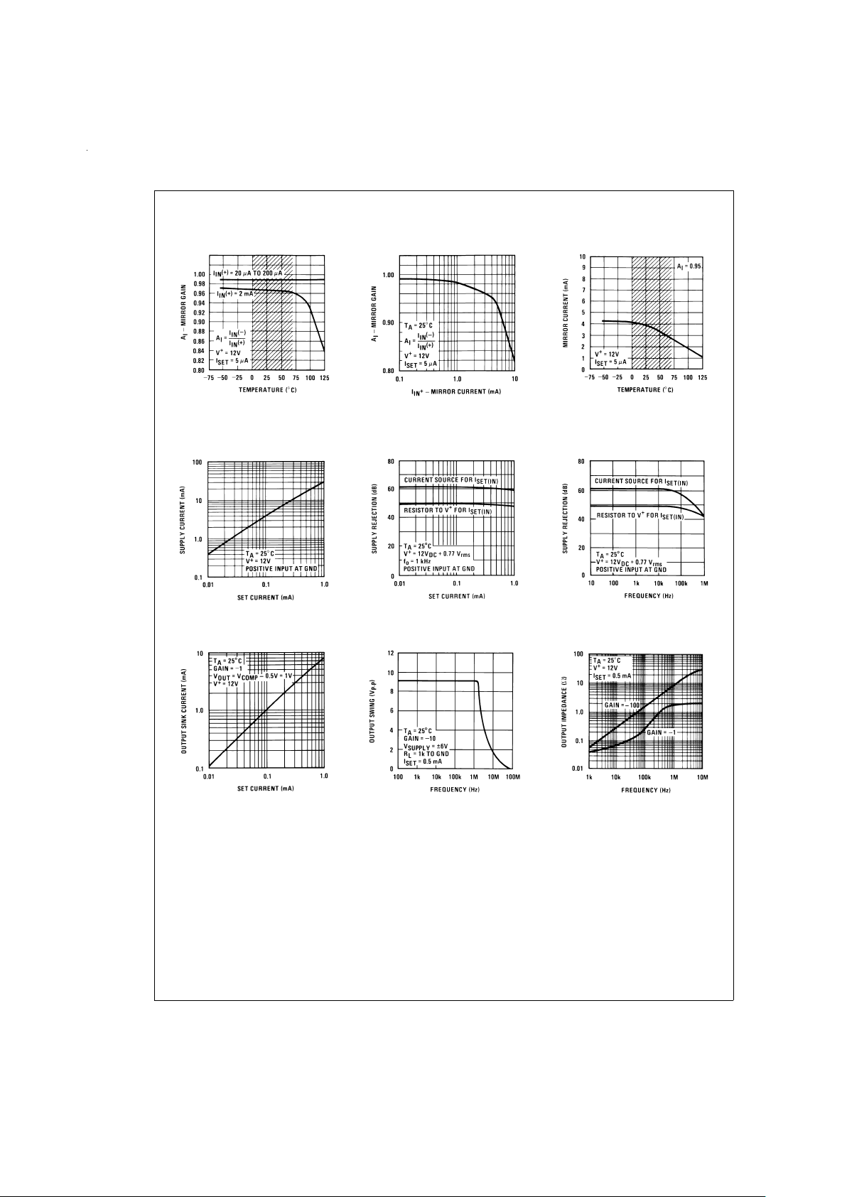
Typical Performance Characteristics (Continued)
Mirror Gain
DS007788-48
Note: Shaded area refers to LM359
Mirror Gain
DS007788-49
Mirror Current
DS007788-50
Note: Shaded area refers to LM359
Supply Current
DS007788-51
Supply Rejection
DS007788-52
Supply Rejection
DS007788-53
Output Sink Current
DS007788-54
Output Swing
DS007788-55
Output Impedance
DS007788-56
www.national.com 6
Typical Performance Characteristics (Continued)
Application Hints
The LM359 consists of two wide bandwidth, decompensated
current differencing (Norton) amplifiers. Although similar in
operation to the original LM3900, design emphasis for these
amplifiers has been placed on obtaining much higher frequency performance as illustrated in
Figure 1
.
This significant improvement in frequency response is the
result of using a common-emitter/common-base (cascode)
gain stage which is typical in many discrete and integrated
video and RF circuit designs. Another versatile aspect of
these amplifiers is the ability to externally program many internal amplifier parameters to suit the requirements of a wide
variety of applications in which this type of amplifier can be
used.
DC BIASING
The LM359 is intended for single supply voltage operation
which requires DC biasing of the output. The current mirror
circuitry which provides the non-inverting input for the amplifier also facilitates DC biasing the output. The basic operation of this current mirror is that
the current (both DC and AC)
flowing into the non-inverting input will force an equal
amount of current to flow into the inverting input
. The mirror
gain (A
I
) specification is the measure of how closely these
two currents match. For more details see National Application Note AN-72.
DC biasing of the output is accomplished by establishing a
reference DC current into the (+) input, I
IN
(+), and requiring
the output to provide the (−) input current. This forces the
output DC level to be whatever value necessary (within the
output voltage swing of the amplifier) to provide this DC reference current,
Figure 2
.
The DC input voltage at each input is a transistor V
BE
(≅0.6 VDC) and must be considered for DC biasing. For
most applications, the supply voltage, V
+
, is suitable and
convenient for establishing I
IN
(+). The inverting input bias
current, I
b
(−), is a direct function of the programmable input
stage current (see current programmability section) and to
obtain predictable output DC biasing set I
IN
(+) ≥ 10Ib(−).
Amplifier to Amplifier
Coupling (Input Referred)
DS007788-57
Noise Voltage
DS007788-58
Maximum Power Dissipation
DS007788-59
Note: Shaded area refers to LM359J/LM359N
DS007788-6
FIGURE 1.
DS007788-7
FIGURE 2.
www.national.com7
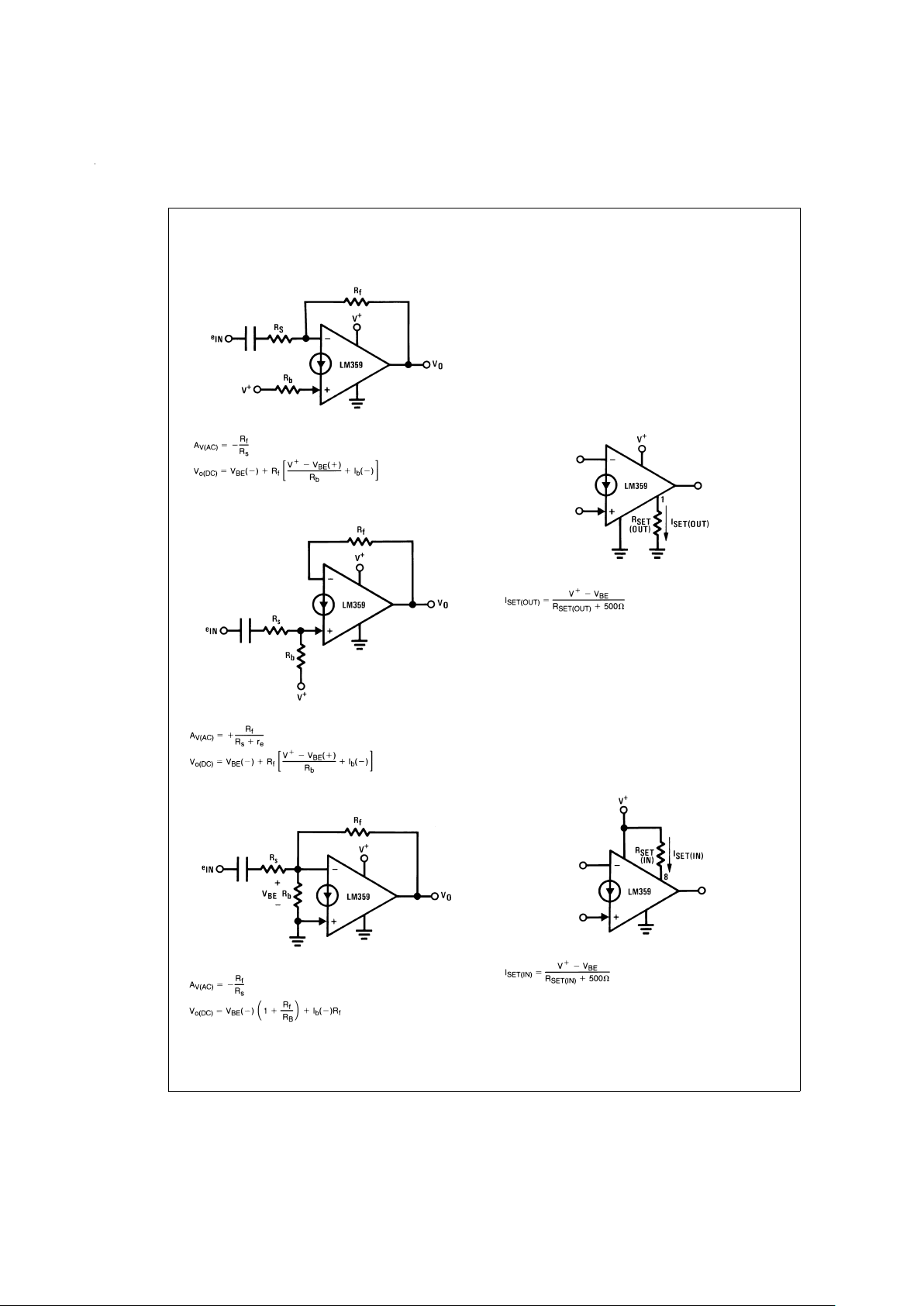
Application Hints (Continued)
The following figures illustrate typical biasing schemes for
AC amplifiers using the LM359:
The nV
BE
biasing configuration is most useful for low noise
applications where a reduced input impedance can be accommodated (see typical applications section).
OPERATING CURRENT PROGRAMMABILITY (I
SET
)
The input bias current, slew rate, gain bandwidth product,
output drive capability and total device power consumption
of both amplifiers can be simultaneously controlled and optimized via the two programming pins I
SET(OUT)
and I
SET(IN)
.
I
SET(OUT)
The output set current (I
SET(OUT)
) is equal to the amount of
current sourced from pin 1 and establishes the class A biasing current for the Darlington emitter follower output stage.
Using a single resistor from pin 1 to ground, as shown in
Fig-
ure 6
, this current is equal to:
The output set current can be adjusted to optimize the
amount of current the output of the amplifier can sink to drive
load capacitance and for loads connected to V
+
.
The maximum output sinking current is approximately 10 times
I
SET(OUT)
. This set current is best used to reduce the total
device supply current if the amplifiers are not required to
drive small load impedances.
I
SET(IN)
The input set current I
SET(IN)
is equal to the current flowing
into pin 8. A resistor from pin 8 to V
+
sets this current to be:
I
SET(IN)
is most significant in controlling the AC characteristics of the LM359 as it directly sets the total input stage current of the amplifiers which determines the maximum slew
rate, the frequency of the open loop dominant pole, the input
resistance of the (−) input and the biasing current I
b
(−).All of
DS007788-8
FIGURE 3. Biasing an Inverting AC Amplifier
DS007788-9
FIGURE 4. Biasing a Non-Inverting AC Amplifier
DS007788-10
FIGURE 5. nVBEBiasing
DS007788-11
FIGURE 6. Establishing the Output Set Current
DS007788-12
FIGURE 7. Establishing the Input Set Current
www.national.com 8
 Loading...