

LM1578A/LM2578A/LM3578A
Switching Regulator
General Description
The LM1578A is a switching regulator which can easily be
set up for such DC-to-DC voltage conversion circuits as the
buck, boost, and inverting configurations. The LM1578A features a unique comparator input stage which not only has
separate pins for both the inverting and non-inverting inputs,
but also provides an internal 1.0V reference to each input,
thereby simplifying circuit design and p.c. board layout. The
output can switch up to 750 mA and has output pins for its
collector and emitter to promote design flexibility.An external
current limit terminal may be referenced to either the ground
or the V
in
terminal, depending upon the application. In addition, the LM1578A has an on board oscillator,which sets the
switching frequency with a single external capacitor from
<
1
Hz to 100 kHz (typical).
The LM1578A is an improved version of the LM1578, offer-
ing higher maximum ratings for the total supply voltage and
output transistor emitter and collector voltages.
Features
n Inverting and non-inverting feedback inputs
n 1.0V reference at inputs
n Operates from supply voltages of 2V to 40V
n Output current up to 750 mA, saturation less than 0.9V
n Current limit and thermal shut down
n Duty cycle up to 90
%
Applications
n Switching regulators in buck, boost, inverting, and
single-ended transformer configurations
n Motor speed control
n Lamp flasher
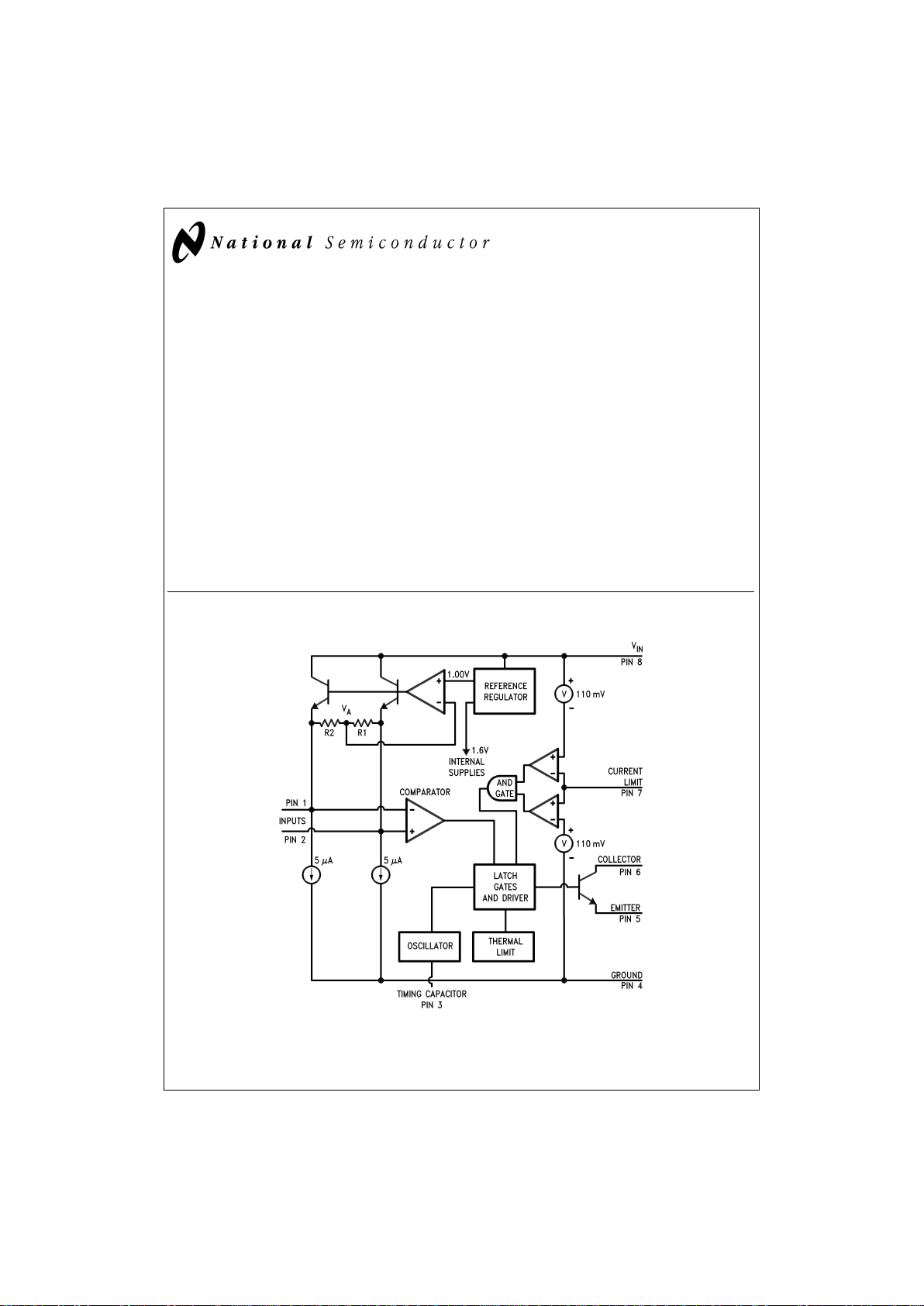
Functional Diagram
DS008711-1
April 1998
LM1578A/LM2578A/LM3578A Switching Regulator
© 1998 National Semiconductor Corporation DS008711 www.national.com
Absolute Maximum Ratings (Note 1)
If Military/Aerospace specified devices are required,
please contact the National Semiconductor Sales Office/
Distributors for availability and specifications.
Total Supply Voltage 50V
Collector Output to Ground −0.3V to +50V
Emitter Output to Ground (Note 2) −1V to +50V
Power Dissipation (Note 3) Internally limited
Output Current 750 mA
Storage Temperature −65˚C to +150˚C
Lead Temperature
(soldering, 10 seconds) 260˚C
Maximum Junction Temperature 150˚C
ESD Tolerance (Note 4) 2 kV
Operating Ratings
Ambient Temperature Range
LM1578A −55˚C ≤ T
A
≤+125˚C
LM2578A −40˚C ≤ T
A
≤+85˚C
LM3578A 0˚C ≤ T
A
≤+70˚C
Junction Temperature Range
LM1578A −55˚C ≤ T
J
≤+150˚C
LM2578A −40˚C ≤ T
J
≤+125˚C
LM3578A 0˚C ≤ T
J
≤+125˚C
Electrical Characteristics
These specifications apply for 2V ≤ VIN≤ 40V (2.2V ≤ VIN≤ 40V for TJ≤ −25˚C), timing capacitor C
T
=
3900 pF, and 25%≤
duty cycle ≤ 75%, unless otherwise specified. Values in standard typeface are for T
J
=
25˚C; values in boldface type apply for
operation over the specified operating junction temperature range.
LM1578A LM2578A/
Symbol Parameter Conditions Typical Limit LM3578A Units
(Note 5) (Note 6)
(Note 11)
Limit
(Note 7)
OSCILLATOR
f
OSC
Frequency 20 kHz
22.4 24 kHz (max)
17.6 16 kHz (min)
∆f
OSC
/∆T Frequency Drift with −0.13
%
/˚C
Temperature
Amplitude 550 mV
p-p
REFERENCE/COMPARATOR (Note 8)
V
R
Input Reference I
1
=
I
2
=
0 mA and 1.0 V
Voltage I
1
=
I
2
=
1mA
±
1%(Note 9) 1.035/1.050 1.050/1.070 V (max)
0.965/0.950 0.950/0.930 V (min)
∆V
R
/∆VINInput Reference Volt- I
1
=
I
2
=
0 mA and 0.003
%
/V
age Line Regulation I
1
=
I
2
=
1mA
±
1%(Note 9) 0.01/0.02 0.01/0.02%/V (max)
I
INV
Inverting Input I
1
=
I
2
=
0 mA, duty cycle=25
%
0.5 µA
Current
Level Shift Accuracy Level Shift Current=1 mA 1.0
%
5/8 10/13
%
(max)
∆V
R
/∆t Input Reference 100 ppm/1000h
Voltage Long Term
Stability
OUTPUT
V
C
(sat) Collector Saturation I
C
=
750 mA pulsed, Emitter 0.7 V
Voltage grounded 0.85/1.2 0.90/1.2 V (max)
V
E
(sat) Emitter Saturation I
O
=
80 mA pulsed, 1.4 V
Voltage V
IN
=
V
C
=
40V 1.6/2.1 1.7/2.0 V (max)
I
CES
Collector Leakage V
IN
=
V
CE
=
40V, Emitter 0.1 µA
Current grounded, Output OFF 50/100 200/250 µA (max)
BV
CEO(SUS)
Collector-Emitter I
SUST
=
0.2A (pulsed), V
IN
=
060 V
Sustaining Voltage 50 50 V (min)
www.national.com 2
Electrical Characteristics (Continued)
These specifications apply for 2V ≤ VIN≤ 40V (2.2V ≤ VIN≤ 40V for TJ≤ −25˚C), timing capacitor C
T
=
3900 pF, and 25%≤
duty cycle ≤ 75%, unless otherwise specified. Values in standard typeface are for T
J
=
25˚C; values in boldface type apply for
operation over the specified operating junction temperature range.
LM1578A LM2578A/
Symbol Parameter Conditions Typical Limit LM3578A Units
(Note 5) (Note 6)
(Note 11)
Limit
(Note 7)
CURRENT LIMIT
V
CL
Sense Voltage Referred to VINor Ground 110 mV
Shutdown Level (Note 10) 95 80 mV (min)
140 160 mV (max)
∆V
CL
/∆T Sense Voltage 0.3
%
/˚C
Temperature Drift
I
CL
Sense Bias Current Referred to V
IN
4.0 µA
Referred to ground 0.4 µA
DEVICE POWER CONSUMPTION
I
S
Supply Current Output OFF, V
E
=
0V 2.0 mA
3.0/3.3 3.5/4.0 mA (max)
Output ON, I
C
=
750 mA pulsed, 14 mA
V
E
=
0V
Note 1: Absolute Maximum Ratings indicate limits beyond which damage to the device may occur. DC andAC electrical specifications do not apply when operating
the device beyond its rated operating conditions.
Note 2: For T
J
≥ 100˚C, the Emitter pin voltage should not be driven more than 0.6V below ground (see Application Information).
Note 3: At elevated temperatures, devices must be derated based on package thermal resistance. The device in the TO-99 package must be derated at 150˚C/W,
junction to ambient, or 45˚C/W,junction tocase. The device inthe 8-pinDIP must be deratedat 95˚C/W,junction to ambient. The device in the surface-mount package
must be derated at 150˚C/W, junction-to-ambient.
Note 4: Human body model, 1.5 kΩ in series with 100 pF.
Note 5: Typical values are for T
J
=
25˚C and represent the most likely parametric norm.
Note 6: All limits guaranteed and 100%production tested at room temperature (standard type face) and at temperature extremes (bold type face). All limits are used
to calculate Average Outgoing Quality Level (AOQL).
Note 7: All limits guaranteed at room temperature (standard type face) and at temperature extremes (bold type face). Room temperature limits are 100%production
tested. Limits at temperatureextremes are guaranteed via correlationusing standard Statistical Quality Control (SQC) methods.All limitsare used to calculateAOQL.
Note 8: Input terminals are protected from accidental shorts to ground but if external voltages higher than the reference voltage are applied, excessive current will
flow and should be limited to less than 5 mA.
Note 9: I
1
and I2are the external sink currents at the inputs (refer to Test Circuit).
Note 10: Connection ofa 10 kΩ resistor frompin 1 to pin 4will drive the duty cycle to its maximum, typically 90%.Applying the minimum Current Limit Sense Voltage
to pin 7 will not reduce the duty cycle to less than 50%. Applying the maximum Current Limit Sense Voltage to pin 7 is certain to reduce the duty cycle below 50%.
Increasing this voltage by 15 mV may be required to reduce the duty cycle to 0%, when the Collector output swing is 40V or greater (see Ground-Referred Current
Limit Sense Voltage typical curve).
Note 11: Amilitary RETS specification is available on request.At the time of printing, the LM1578ARETS spec complied with the boldface limits in this column. The
LM1578AH may also be procured as a Standard Military Drawing.
3 www.national.com
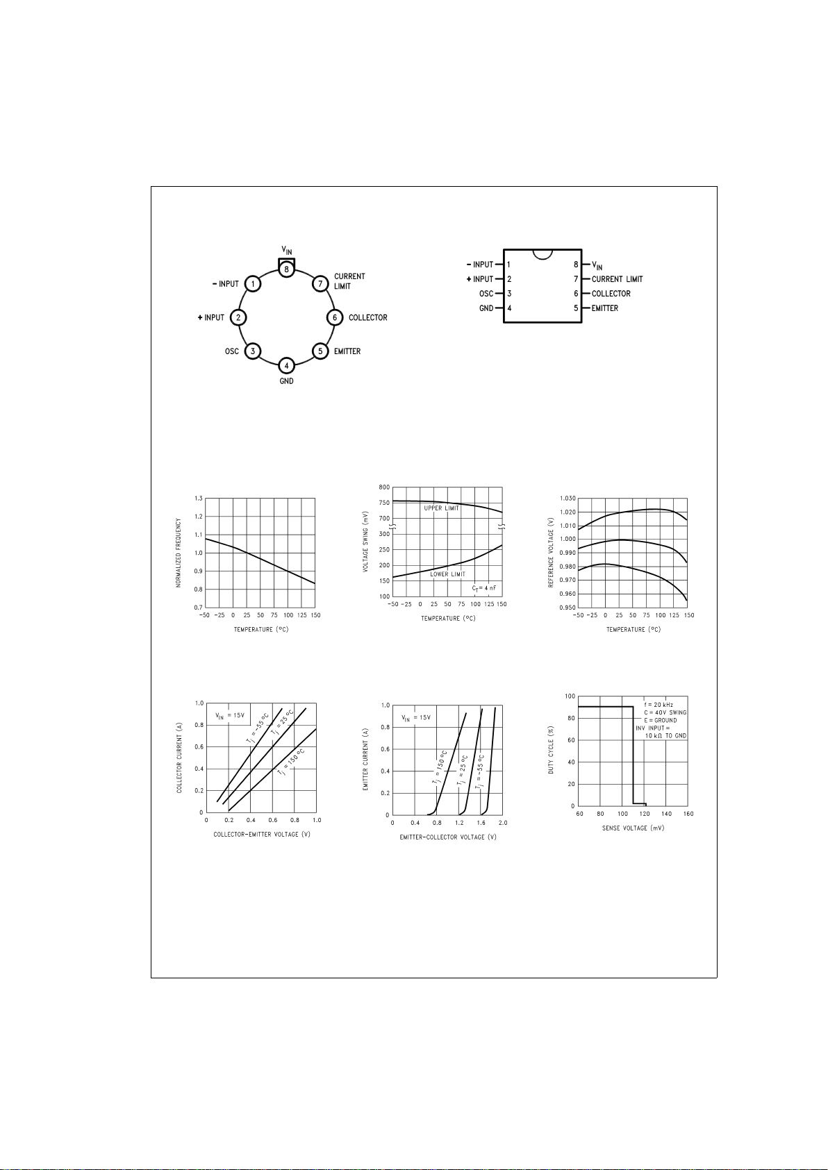
Connection Diagram and Ordering Information
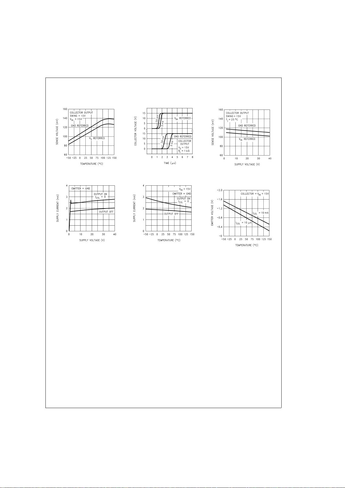
Typical Performance Characteristics
Metal Can
DS008711-28
Top View
Order Number LM1578AH/883 or SMD
#
5962-8958602
See NS Package Number H08C
Dual-In-Line Package
DS008711-29
Order Number LM3578AM, LM2578AN or LM3578AN
See NS Package Number M08A or N08E
Oscillator Frequency Change
with Temperature
DS008711-32
Oscillator Voltage Swing
DS008711-33
Input Reference Voltage
Drift with Temperature
DS008711-34
Collector Saturation Voltage
(Sinking Current,
Emitter Grounded)
DS008711-35
Emitter Saturation Voltage
(Sourcing Current,
Collector at V
in
)
DS008711-36
Ground Referred
Current Limit Sense Voltage
DS008711-37
www.national.com 4
Typical Performance Characteristics (Continued)
Test Circuit
*
Parameter tests can be made using the test circuit shown.
Select the desired V
in
, collector voltage and duty cycle with
adjustable power supplies. A digital volt meter with an input
resistance greater than 100 MΩ should be used to measure
the following:
Input Reference Voltage to Ground; S1 in either position.
Level Shift Accuracy (%)=(T
P3
(V)/1V) x 100%;S1atI
1
=
I
2
=
1mA
Input Current (mA)=(1V − T
p3
(V))/1 MΩ:S1atI
1
=
I
2
=
0 mA.
Oscillator parameters can be measured at T
p4
using a fre-
quency counter or an oscilloscope.
The Current Limit Sense Voltage is measured by connecting
an adjustable 0-to-1V floating power supply inseries with the
current limit terminal and referring it to either the ground or
the V
in
terminal. Set the duty cycle to 90%and monitor test
point T
P5
while adjusting the floating power supply voltage
until the LM1578A’s duty cycle just reaches 0%. This voltage
is the Current Limit Sense Voltage.
The Supply Current should be measured with the duty cycle
at 0%and S1 in the I
1
=
I
2
=
0 mA position.
*
LM1578A specifications are measured using automated
test equipment. This circuit is provided for the customer’s
convenience when checking parameters. Due to possible
variations in testing conditions, the measured values from
these testing procedures may not match those of the factory.
Current Limit Sense Voltage
Drift with Temperature
DS008711-38
Current Limit Response Time
for Various Over Drives
DS008711-39
Current Limit Sense Voltage
vs Supply Voltage
DS008711-40
Supply Current
DS008711-41
Supply Current
DS008711-42
Collector Current with
Emitter Output Below Ground
DS008711-43
5 www.national.com
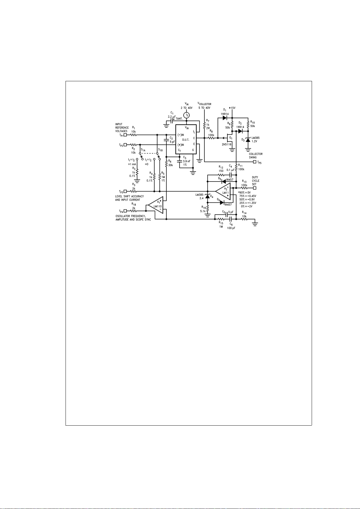
Test Circuit
*
(Continued)
Definition of Terms
Input Reference Voltage: The voltage (referred to ground)
that must be applied to either the inverting or non-inverting
input to cause the regulator switch to change state (ON or
OFF).
Input Reference Current: The current that must be drawn
from either the inverting or non-inverting input to cause the
regulator switch to change state (ON or OFF).
Input Level Shift Accuracy: This specification determines
the output voltagetolerance of a regulator whose output control depends on drawing equal currents from the inverting
and non-inverting inputs (see the Inverting Regulator of
Fig-
ure 21
, and the RS-232 Line Driver Power Supply of
Figure
23
).
Level Shift Accuracy is tested by using two equal-value resistors to draw current from the inverting and non-inverting
input terminals, then measuring the percentage difference in
the voltages across the resistors that produces a controlled
duty cycle at the switch output.
Collector Saturation Voltage: With the inverting input terminal grounded thru a 10 kΩ resistor and the output transistor’s emitter connected to ground, the Collector SaturationVoltage is the collector-to-emitter voltage for a given
collector current.
Emitter Saturation Voltage: With the inverting input terminal grounded thru a 10kΩ resistor and the output transistor’s
collector connected to V
in
, the Emitter Saturation Voltage is
the collector-to-emitter voltage for a given emitter current.
Collector Emitter Sustaining Voltage: The
collector-emitter breakdown voltage of the output transistor,
measured at a specified current.
Current Limit Sense Voltage: The voltage at the Current
Limit pin, referred to either the supply or the ground terminal,
which (via logic circuitry) will cause the output transistor to
turn OFF and resets cycle-by-cycle at the oscillator frequency.
Current Limit Sense Current: The bias current for the Current Limit terminal with the applied voltage equal to the Current Limit Sense Voltage.
Supply Current: The IC power supply current, excluding the
current drawn through the output transistor, with the oscillator operating.
Functional Description
The LM1578A is a pulse-width modulator designed for use
as a switching regulator controller. It may also be used in
other applications which require controlled pulse-width voltage drive.
Acontrol signal, usually representing output voltage, fed into
the LM1578A’s comparator is compared with an
internally-generated reference. The resulting error signal
and the oscillator’s output are fed to a logic network which
determines when the output transistor will be turned ON or
OFF. The following isa brief description of the subsections of
the LM1578A.
COMPARATOR INPUT STAGE
The LM1578A’s comparator input stage is unique in that
both the inverting and non-inverting inputs are available to
the user, and both contain a 1.0V reference. This is accomplished as follows: A 1.0V reference is fed into a modified
voltage follower circuit (see FUNCTIONAL DIAGRAM).
When both input pins are open, no current flows through R1
DS008711-3
Op amp supplies are±15V
DVM input resistance
>
100 MΩ
*
LM1578 max duty cycle is 90
%
www.national.com 6
 Loading...