

NSC LM3526M-L, LM3526M-H, LM3526MX-L Datasheet
LM3526
Dual Port USB Power Switch and Over-Current
Protection
LM3526 Dual Port USB Power Switch and Over-Current Protection
February 2000
General Description
The LM3526 provides Universal Serial Bus standard power
switch and over-current protection for all host port applications. The dual port device is ideal for Notebook and desktop
PC’s that supply power to more than one port.
A 1 ms delay on the fault flag output prevents erroneous
overcurrent reporting caused by in-rush currents during
hot-plug events.
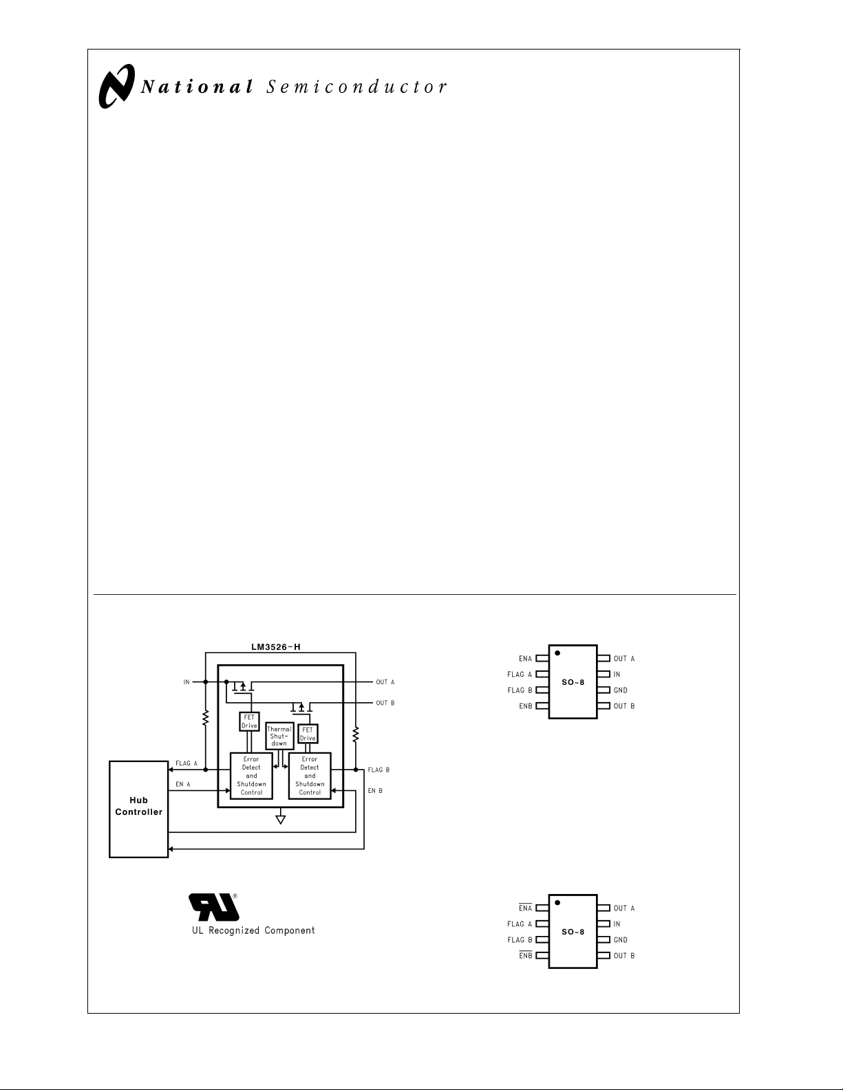
The dual stage thermal protection circuit in the LM3526 provides individual protection to each switch and the entire device. In a short-circuit/over-current event, the switch dissipating excessive heat is turned off, allowing the second switch
to continue to function uninterrupted.
The LM3526 accepts an input voltage between 2.7V and
5.5V allowing use as a device-based in-rush current limiter
for 3.3V USB peripherals, as well as Root and Self-Powered
Hubs at 5.5V. The Enable inputs accept both 3.3V and 5.0V
logic thresholds.
The small size, low R
LM3526 a good choice for root hubs as well as per-port
power control in embedded and stand-alone hubs.
, and 1 ms fault flag delay make the
ON
Features
n 1 ms fault flag delay filters Hot-Plug events
n Smooth turn-on eliminates in-rush induced voltage drop
n UL recognized component: REF
n 1A nominal short circuit output current protects PC
power supplies
n Thermal shutdown protects device in direct short
condition
n 500mA minimum continuous load current
n Small SO-8 package minimizes board space
n 2.7V to 5.5V input voltage range
n 140 mΩ Max. switch resistance
n 1 µA Max. standby current
n 200 µA Max. operating current
n Under-voltage lockout (UVLO)
Applications
n Universal Serial Bus (USB) Root Hubs including
Desktop and Notebook PC
n USB Monitor Hubs
n Other Self-Powered USB Hub Devices
n High Power USB Devices Requiring In-rush Limiting
n General Purpose High Side Switch Applications
Typical Operating Circuit and Connection Diagram
#
205202
DS101097-2
LM3526-H
DS101097-1
DS101097-40
DS101097-28
LM3526-L
© 2000 National Semiconductor Corporation DS101097 www.national.com
Ordering Information
LM3526
Part Number Enable, Delivery Option Package Type
LM3526M-H Active High Enable, 95 units per rail
LM3526M-L Active Low Enable, 95 units per rail
LM3526MX-H Active High Enable, 2500 units per reel
LM3526MX-L Active Low Enable, 2500 units per reel
SO-8,
NS Package
Number M08A
www.national.com 2
LM3526
Absolute Maximum Ratings (Note 1)
If Military/Aerospace specified devices are required,
please contact the National Semiconductor Sales Office/
Distributors for availability and specifications.
Supply Voltage −0.3V to 6V
Output Voltage −0.3V to 6V
Voltage at All Other Pins −0.3V to 5.5V
Power Dissipation (T
(Note 2) 700 mW
T
(Note 2) 160˚C
JMAX
= 25˚C)
A
Operating Ratings
Supply Voltage Range 2.7V to 5.5V
Operating Ambient Range −40˚C to 85˚C
Operating Junction Temperature
Range −40˚C to 125˚C
Storage Temperature Range −65˚C to +150˚C
Lead Temperature
(Soldering, 5 seconds) 260˚C
ESD Rating (Note 3)
ESD Rating Output Only
2kV
8kV
DC Electrical Characteristics
Limits in standard typeface are for T
less otherwise specified: V
=
IN
Symbol Parameter Conditions Min Typ Max Units
R
I
ON
OUT
On Resistance
OUT pins continuous
output current
I
SC
Short Circuit Output
Current
OC
I
LEAK
THRESH
Over-current Threshold 2.2 3.2 A
OUT pins Output
Leakage Current
R
I
V
V
V
FO
EN
IH
IL
UVLO
FLAG Output Voltage
EN/EN Leakage Current VEN/VEN=0VorVEN/VEN=V
EN/EN Input Logic High (Note 5) 2.4 1.9 V
EN/EN Input Logic Low (Note 5) 1.7 0.8 V
Under-Voltage Lockout
Threshold
I
DDOFF
I
DDON
Th
SD
Supply Current Switch-Off
Supply Current Switch-On 115 200 µA
Over-temperature
Shutdown Threshold
I
FH
Error Flag Leakage
Current
Note 1: Absolute Maximum Ratings indicate limits beyond which damage to the device may occur. Electrical specifications do not apply when operating the device
beyond its rated operating conditions.
Note 2: The maximum power dissipation must be derated at elevated temperatures and is dictated by T
bient thermal resistance), andT
given in the Absolute Maximum Ratings, which ever is lower. θ
Note 3: The human body model is a 100 pF capacitor discharged through a 1.5 kΩ resistor into each pin. Enable pin ESD threshold is 1.7kV.
Note 4: Thermal Shutdown will protect the device from permanent damage.
Note 5: For LM3526-L, OFF is EN ≥ 2.4V and ON is EN ≤ 0.8V. For LM3526-H, OFF is EN ≤ 0.8V and ON is EN ≥ 2.4V.
(ambient temperature). The maximumallowablepower dissipation at any temperature is P
A
J
5.0V, V
=
25˚C, and limits in boldface type apply over the full operating temperature range. Un-
=
0V (LM3526-L) or V
EN
=
V
5V, I
IN
=
2.7V, I
V
IN
=
500mA, each switch 100 140
OUT
=
OUT
=
(LM3526-H).
V
EN
IN
500mA, each switch 110 180
Each Output 0.5 A
Each Output (enable into Load) (Note 4)
=
OUT
OUT
=
4.0V
0.1V
V
V
VEN=VIN(LM3526-L)
0.5 1.2
1
0.01 10 µA
1.9
1.5
VEN= 0V (LM3526-H)
= 10 mA, V
I
FO
= 10 mA, V
FO
I
= 10 mA, V
FO
=
5.0V 10 25
IN
=
3.3V 11 35
IN
=
2.7V 12 40
IN
IN
−0.5 0.5 µA
1.8 V
0.2 1
−40˚C ≤ T
TJIncreasing, with no shorted output
Increasing, with shorted output (s)
T
J
Decreasing (Note 4)
T
J
V
flag
≤ 85˚C
J
150
145
135
=
5V 0.01 1 µA
(Maximum junction temperature), θJA(junction to am-
JA
=
150˚C/W.
JMAX
DMAX
=
(T
JMAX−TA
2
)/θJAor the number
mΩ
A
ΩI
µA
˚C
www.national.com3
AC Electrical Characteristics
Limits in standard typeface are for T
LM3526
less otherwise specified: V
=
IN
Symbol Parameter Conditions Min Typ Max Units
t
r
t
f
t
ON
t
OFF
t
OC
OUT Rise Time RL=10Ω 100 µs
OUT Fall Time RL=10Ω 5µs
Turn on Delay, EN to OUT RL=10Ω 150 µs
Turn off Delay, EN to OUT RL=10Ω 5µs
Over Current Flag Delay RL=0 1 ms
5.0V.
=
25˚C, and limits in boldface type apply over the full operating temperature range. Un-
J
Pin Description
Pin Number Pin Name Pin Function
1, 4 ENA, ENB
(LM3526-L)
ENA, ENB
(LM3526-H)
2, 3 FLAG A
FLAG B
6 GND Ground
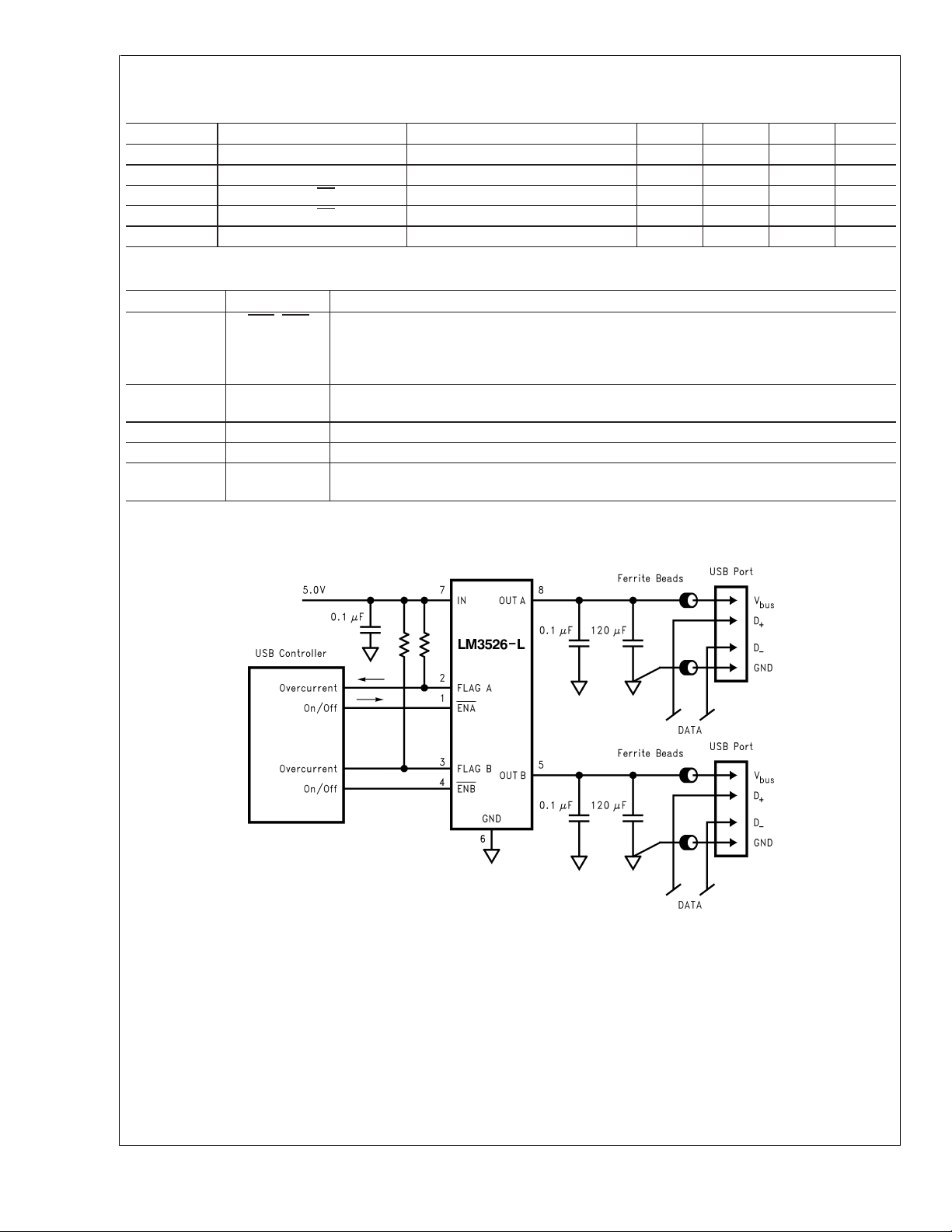
7 IN Supply Input: This pin is the input to the power switch and the supply voltage for the IC.
8, 5 OUT A
OUT B
Enable (Input): Logic-compatible enable inputs.
Fault Flag (Output): Active-low, open-drain outputs. Indicates overcurrent, UVLO or thermal
*
shutdown.
See application section for more information.
Switch Output: These pins are the outputs of the high side switch.
Typical Application Circuit
DS101097-3
www.national.com 4
 Loading...