NSC LM34CZ, LM34CH, LM34CAZ, LM34DZ, LM34DMDC Datasheet
...
LM34
Precision Fahrenheit Temperature Sensors
General Description
The LM34 series are precision integrated-circuit temperature
sensors, whose output voltage is linearly proportional to the
Fahrenheit temperature. The LM34 thus has an advantage
over linear temperature sensors calibrated in degrees
Kelvin, as the user is not required to subtract a large constant voltage from its output to obtain convenient Fahrenheit
scaling. The LM34 does not require any external calibration
or trimming to provide typical accuracies of
±
1
⁄2˚F at room
temperature and
±
11⁄2˚F over a full −50 to +300˚F temperature range. Low cost is assured by trimming and calibration
at the wafer level. The LM34’s low output impedance, linear
output, and precise inherent calibration make interfacing to
readout or control circuitry especially easy. It can be used
with single power supplies or with plus and minus supplies.
As it draws only 75 µA from its supply, it has very low
self-heating, less than 0.2˚F in still air. The LM34 is rated to
operate over a −50˚ to +300˚F temperature range, while the
LM34C is rated for a −40˚ to +230˚F range (0˚F with improved accuracy). The LM34 series is available packaged in
hermetic TO-46 transistor packages, while the LM34C,
LM34CA and LM34D are also available in the plastic TO-92
transistor package. The LM34D is also available in an8-lead
surface mount small outline package.TheLM34isacomplement to the LM35 (Centigrade) temperature sensor.
Features
n Calibrated directly in degrees Fahrenheit
n Linear +10.0 mV/˚F scale factor
n 1.0˚F accuracy guaranteed (at +77˚F)
n Rated for full −50˚ to +300˚F range
n Suitable for remote applications
n Low cost due to wafer-level trimming
n Operates from 5 to 30 volts
n Less than 90 µA current drain
n Low self-heating, 0.18˚F in still air
n Nonlinearity only
±
0.5˚F typical
n Low-impedance output, 0.4Ω for 1 mA load
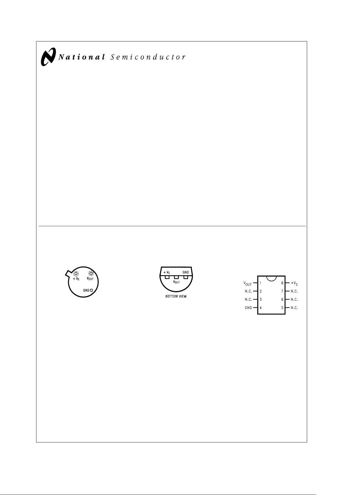
Connection Diagrams
Note 1: Case is connected to negative pin (GND).
TO-46
Metal Can Package
(Note 1)
DS006685-1
Order Numbers LM34H,
LM34AH, LM34CH,
LM34CAH or LM34DH
See NS Package
Number H03H
TO-92
Plastic Package
DS006685-2
Order Number LM34CZ,
LM34CAZ or LM34DZ
See NS Package
Number Z03A
SO-8
Small Outline
Molded Package
DS006685-20
N.C. = No Connection
Top View
Order Number LM34DM
See NS Package Number M08A
November 2000
LM34 Precision Fahrenheit Temperature Sensors
© 2000 National Semiconductor Corporation DS006685 www.national.com

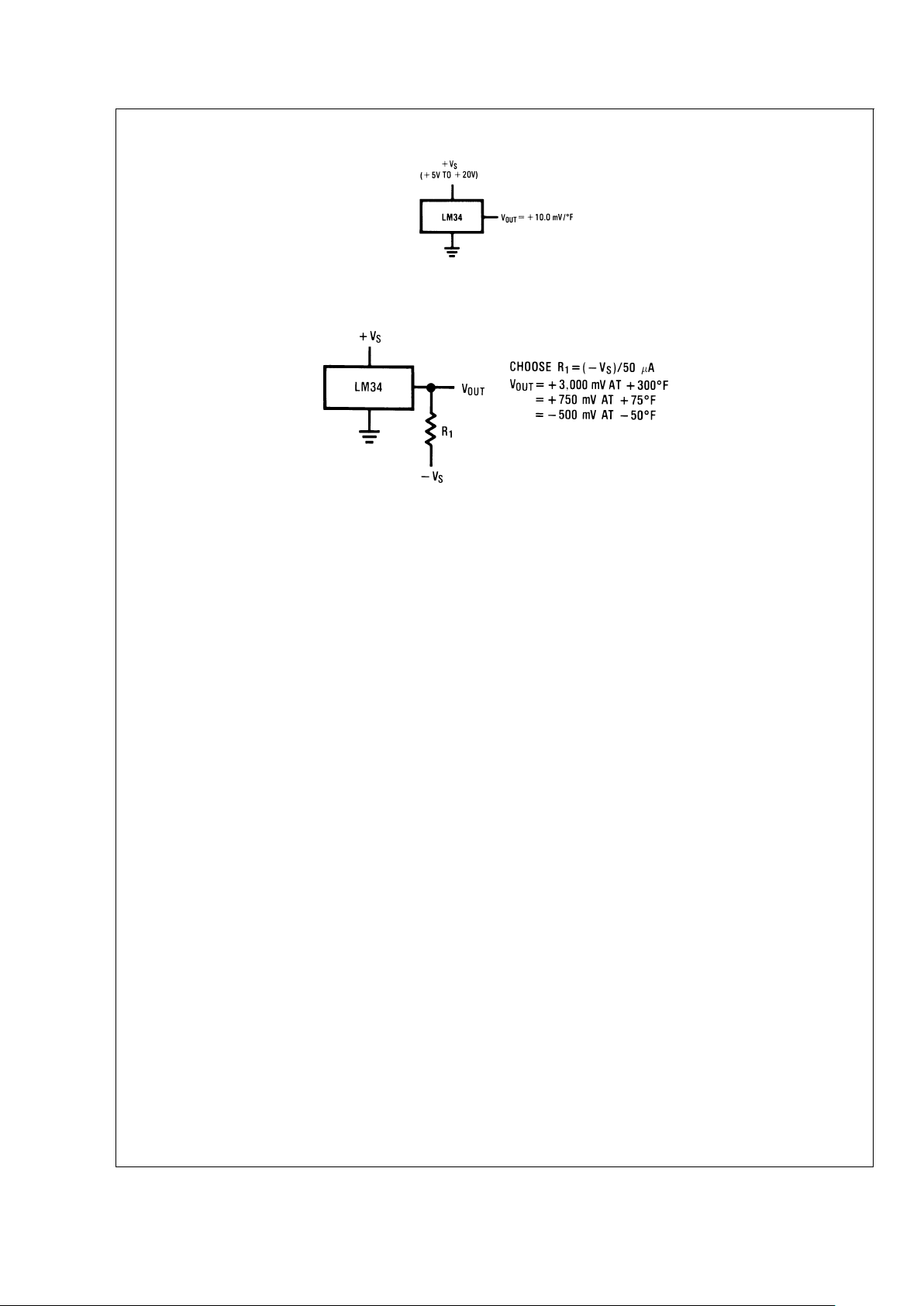
Typical Applications
DS006685-3
FIGURE 1. Basic Fahrenheit Temperature Sensor
(+5˚ to +300˚F)
DS006685-4
FIGURE 2. Full-Range Fahrenheit Temperature Sensor
LM34
www.national.com 2

Absolute Maximum Ratings (Note 11)
If Military/Aerospace specified devices are required,
please contact the National Semiconductor Sales Office/
Distributors for availability and specifications.
Supply Voltage +35V to −0.2V
Output Voltage +6V to −1.0V
Output Current 10 mA
Storage Temperature,
TO-46 Package −76˚F to +356˚F
TO-92 Package −76˚F to +300˚F
SO-8 Package −65˚C to +150˚C
ESD Susceptibility (Note 12) 800V
Lead Temp.
TO-46 Package
(Soldering, 10 seconds) +300˚C
TO-92 Package
(Soldering, 10 seconds) +260˚C
SO Package (Note 13)
Vapor Phase (60 seconds) 215˚C
Infrared (15 seconds) 220˚C
Specified Operating Temp. Range (Note 3)
T
MIN
to T
MAX
LM34, LM34A −50˚F to +300˚F
LM34C, LM34CA −40˚F to +230˚F
LM34D +32˚F to +212˚F
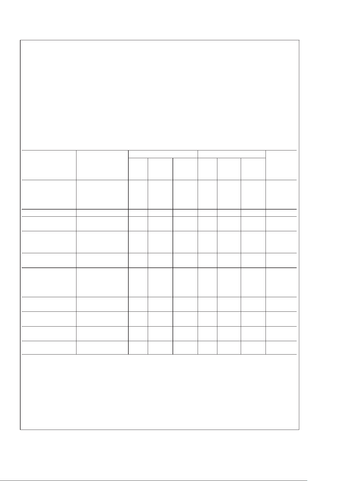
DC Electrical Characteristics (Notes 2, 7)
LM34A LM34CA
Parameter Conditions Tested Design Tested Design Units
Typical Limit Limit Typical Limit Limit (Max)
(Note 5) (Note 6) (Note 5) (Note 6)
Accuracy (Note 8) T
A
= +77˚F
±
0.4
±
1.0
±
0.4
±
1.0 ˚F
T
A
= 0˚F
±
0.6
±
0.6
±
2.0 ˚F
T
A=TMAX
±
0.8
±
2.0
±
0.8
±
2.0 ˚F
T
A=TMIN
±
0.8
±
2.0
±
0.8
±
3.0 ˚F
Nonlinearity (Note 9) T
MIN
≤ TA≤ T
MAX
±
0.35
±
0.7
±
0.30
±
0.6 ˚F
Sensor Gain T
MIN
≤ TA≤ T
MAX
+10.0 +9.9, +10.0 +9.9, mV/˚F, min
(Average Slope) +10.1 +10.1 mV/˚F, max
Load Regulation T
A
= +77˚F
±
0.4
±
1.0
±
0.4
±
1.0 mV/mA
(Note 4) T
MIN
≤ TA≤ T
MAX
±
0.5
±
3.0
±
0.5
±
3.0 mV/mA
0 ≤ I
L
≤ 1mA
Line Regulation T
A
= +77˚F
±
0.01
±
0.05
±
0.01
±
0.05 mV/V
(Note 4) 5V ≤ V
S
≤ 30V
±
0.02
±
0.1
±
0.02
±
0.1 mV/V
Quiescent Current V
S
= +5V, +77˚F 75 90 75 90 µA
(Note 10) V
S
= +5V 131 160 116 139 µA
V
S
= +30V, +77˚F 76 92 76 92 µA
V
S
= +30V 132 163 117 142 µA
Change of Quiescent 4V ≤ V
S
≤ 30V, +77˚F +0.5 2.0 0.5 2.0 µA
Current (Note 4) 5V ≤ V
S
≤ 30V +1.0 3.0 1.0 3.0 µA
Temperature Coefficient +0.30 +0.5 +0.30 +0.5 µA/˚F
of Quiescent Current
Minimum Temperature In circuit of
Figure 1
, +3.0 +5.0 +3.0 +5.0 ˚F
for Rated Accuracy I
L
=0
Long-Term Stability T
j=TMAX
for 1000 hours
±
0.16
±
0.16 ˚F
Note 2: Unless otherwise noted, these specifications apply: −50˚F ≤ Tj≤ + 300˚F for the LM34 and LM34A; −40˚F ≤ Tj≤ +230˚F for the LM34C and LM34CA; and
+32˚F ≤T
j
≤ + 212˚F for the LM34D.VS= +5 Vdc and I
LOAD
= 50 µA in the circuitof
Figure 2
; +6 Vdc for LM34 andLM34A for 230˚F ≤ Tj≤ 300˚F.These specifications
also apply from +5˚F to T
MAX
in the circuit of
Figure 1
.
Note 3: Thermal resistance of the TO-46 package is 720˚F/W junction toambient and 43˚F/W junction to case. Thermal resistance of the TO-92 package is 324˚F/W
junction to ambient. Thermal resistance of the small outline molded package is 400˚F/W junction to ambient. For additional thermal resistance information see table
in the Typical Applications section.
Note 4: Regulation ismeasured atconstant junctiontemperature usingpulse testing with a low duty cycle. Changes in output due to heating effects can be computed
by multiplying the internal dissipation by the thermal resistance.
Note 5: Tested limits are guaranteed and 100% tested in production.
Note 6: Design limits are guaranteed (but not 100% production tested) over the indicated temperature and supply voltage ranges. These limits are not used to
calculate outgoing quality levels.
Note 7: Specification in BOLDFACE TYPE apply over the full rated temperature range.
LM34
www.national.com3

DC Electrical Characteristics (Notes 2, 7) (Continued)
Note 8: Accuracy is defined as the error between the output voltage and 10 mV/˚F times the device’s case temperature at specified conditions of voltage, current,
and temperature (expressed in ˚F).
Note 9: Nonlinearity is defined as the deviation of the output-voltage-versus-temperature curve from the best-fit straight line over the device’s rated temperature
range.
Note 10: Quiescent current is defined in the circuit of
Figure 1
.
Note 11: Absolute Maximum Ratings indicate limits beyond which damage to thedevice may occur. DC and AC electrical specifications do not apply when operating
the device beyond its rated operating conditions (Note 2).
Note 12: Human body model, 100 pF discharged through a 1.5 kΩ resistor.
Note 13: See AN-450 “Surface Mounting Methods and Their Effect on Product Reliability” or the section titled “Surface Mount” found in a current National
Semiconductor Linear Data Book for other methods of soldering surface mount devices.
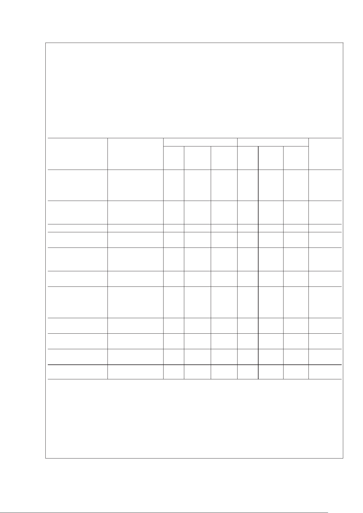
DC Electrical Characteristics (Notes 2, 7)
LM34 LM34C, LM34D
Parameter Conditions Tested Design Tested Design Units
Typical Limit Limit Typical Limit Limit (Max)
(Note 5) (Note 6) (Note 5) (Note 6)
Accuracy, LM34, LM34C T
A
= +77˚F
±
0.8
±
2.0
±
0.8
±
2.0 ˚F
(Note 8) T
A
= 0˚F
±
1.0
±
1.0
±
3.0 ˚F
T
A=TMAX
±
1.6
±
3.0
±
1.6
±
3.0 ˚F
T
A=TMIN
±
1.6
±
3.0
±
1.6
±
4.0 ˚F
Accuracy, LM34D T
A
= +77˚F
±
1.2
±
3.0 ˚F
(Note 8) T
A=TMAX
±
1.8
±
4.0 ˚F
T
A=TMIN
±
1.8
±
4.0 ˚F
Nonlinearity (Note 9) T
MIN
≤ TA≤ T
MAX
±
0.6
±
1.0
±
0.4
±
1.0 ˚F
Sensor Gain T
MIN
≤ TA≤ T
MAX
+10.0 +9.8, +10.0 +9.8, mV/˚F, min
(Average Slope) +10.2 +10.2 mV/˚F, max
Load Regulation T
A
= +77˚F
±
0.4
±
2.5
±
0.4
±
2.5 mV/mA
(Note 4) T
MIN
≤ TA≤ +150˚F
±
0.5
±
6.0
±
0.5
±
6.0 mV/mA
0 ≤ I
L
≤ 1mA
Line Regulation T
A
= +77˚F
±
0.01
±
0.1
±
0.01
±
0.1 mV/V
(Note 4) 5V ≤ V
S
≤ 30V
±
0.02
±
0.2
±
0.02
±
0.2 mV/V
Quiescent Current V
S
= +5V, +77˚F 75 100 75 100 µA
(Note 10) V
S
= +5V 131 176 116 154 µA
V
S
= +30V, +77˚F 76 103 76 103 µA
V
S
= +30V 132 181 117 159 µA
Change of Quiescent 4V ≤ V
S
≤ 30V, +77˚F +0.5 3.0 0.5 3.0 µA
Current (Note 4) 5V ≤ V
S
≤ 30V +1.0 5.0 1.0 5.0 µA
Temperature Coefficient +0.30 +0.7 +0.30 +0.7 µA/˚F
of Quiescent Current
Minimum Temperature In circuit of
Figure 1
, +3.0 +5.0 +3.0 +5.0 ˚F
for Rated Accuracy I
L
=0
Long-Term Stability T
j=TMAX
for 1000 hours
±
0.16
±
0.16 ˚F
LM34
www.national.com 4
 Loading...