

NSC LM34919TL, LM34919 Datasheet
November 1, 2007
LM34919
40V, 600 mA Step Down COT Switching Regulator
General Description
The LM34919 Step Down Switching Regulator features all of
the functions needed to implement a low cost, efficient, buck
bias regulator capable of supplying 0.6A to the load. This buck
regulator contains an N-Channel Buck Switch, and is available in a micro SMD package. The constant on-time feedback
regulation scheme requires no loop compensation, results in
fast load transient response, and simplifies circuit implementation. The operating frequency remains constant with line
and load variations due to the inverse relationship between
the input voltage and the on-time. The valley current limit results in a smooth transition from constant voltage to constant
current mode when current limit is detected, reducing the frequency and output voltage, without the use of foldback. Additional features include: VCC under-voltage lockout, thermal
shutdown, gate drive under-voltage lockout, and maximum
duty cycle limiter.
Features
■
Integrated N-Channel buck switch
■
Integrated start-up regulator
■
Input Voltage Range: 8V to 40V
■
No loop compensation required
■
Ultra-Fast transient response
■
Operating frequency remains constant with load current
and input voltage
■
Maximum switching frequency: 1.6 MHz
■
Maximum Duty Cycle Limited During Start-Up
■
Adjustable output voltage
■
Valley Current Limit At 0.64A
■
Precision internal reference
■
Low bias current
■
Highly efficient operation
■
Thermal shutdown
Typical Applications
■
High Efficiency Point-Of-Load (POL) Regulator
■
Non-Isolated Telecommunication Buck Regulator
■
Secondary High Voltage Post Regulator
Package
■
micro SMD
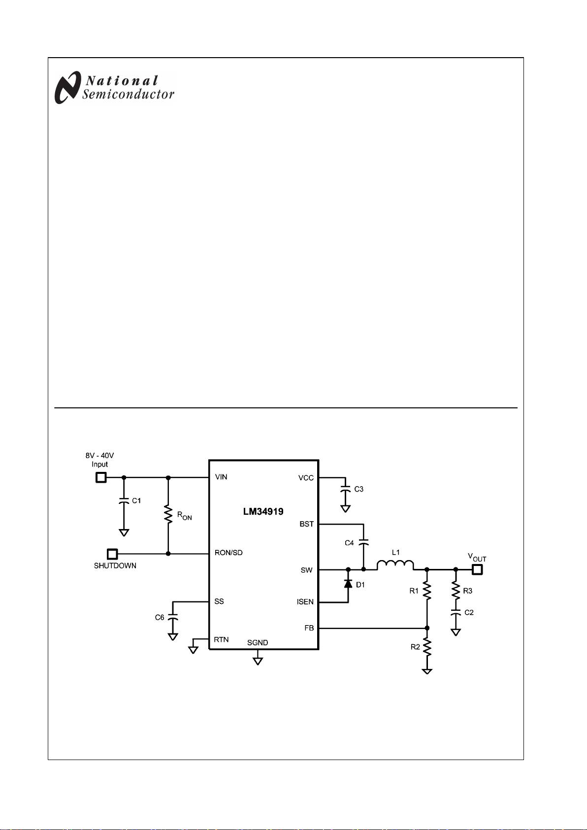
Basic Step Down Regulator
30004431
© 2007 National Semiconductor Corporation 300044 www.national.com
LM34919 40V, 600 mA Step Down COT Switching Regulator
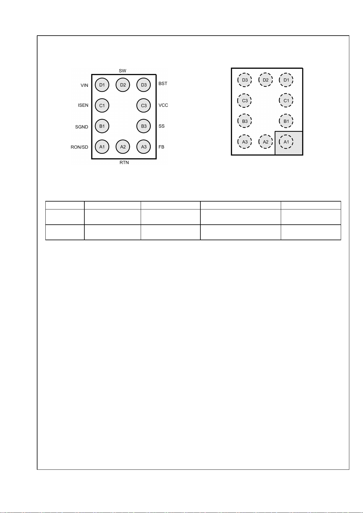
Connection Diagrams
30004402
Bump Side
30004433
Top View
Ordering Information
Order Number Package Type NSC Package Drawing Junction Temperature Range Supplied As
LM34919TL 10-Bump micro SMD TLP10A1A −40°C to + 125°C 250 Units on Tape and
Reel
LM34919TLX 10-Bump micro SMD TLP10A1A −40°C to + 125°C 3000 Units on Tape and
Reel
www.national.com 2
LM34919
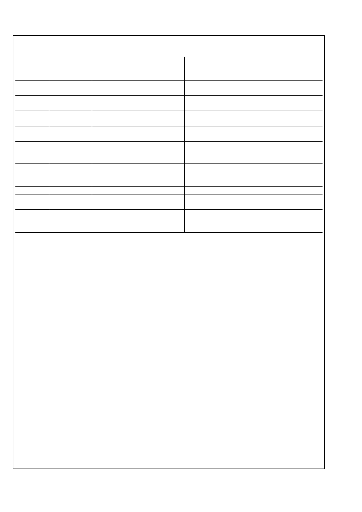
Pin Descriptions
Pin Number Name Description Application Information
A1 RON/SD On-time control and shutdown An external resistor from VIN to this pin sets the buck switch
on-time. Grounding this pin shuts down the regulator.
A2 RTN Circuit Ground Ground for all internal circuitry other than the current limit
detection.
A3 FB Feedback input from the regulated
output
Internally connected to the regulation and over-voltage
comparators. The regulation level is 2.5V.
B1 SGND Sense Ground Re-circulating current flows into this pin to the current sense
resistor.
B3 SS Softstart An internal current source charges an external capacitor to
2.5V, providing the softstart function.
C1 ISEN Current sense The re-circulating current flows through the internal sense
resistor, and out of this pin to the free-wheeling diode.
Current limit is nominally set at 0.64A.
C3 VCC Output from the startup regulator Nominally regulates at 7.0V. An external voltage (7V-14V)
can be applied to this pin to reduce internal dissipation. An
internal diode connects VCC to VIN.
D1 VIN Input supply voltage Nominal input range is 8.0V to 40V.
D2 SW Switching Node Internally connected to the buck switch source. Connect to
the inductor, free-wheeling diode, and bootstrap capacitor.
D3 BST Boost pin for bootstrap capacitor Connect a 0.022 µF capacitor from SW to this pin. The
capacitor is charged from VCC via an internal diode during
each off-time.
3 www.national.com
LM34919
Absolute Maximum Ratings (Note 1)
If Military/Aerospace specified devices are required,
please contact the National Semiconductor Sales Office/
Distributors for availability and specifications.
VIN to RTN 44V
BST to RTN 52V
SW to RTN (Steady State) -1.5V
ESD Rating (Note 2)
Human Body Model 2kV
BST to VCC 44V
VIN to SW 44V
BST to SW 14V
VCC to RTN 14V
SGND to RTN -0.3V to +0.3V
SS to RTN -0.3V to 4V
All Other Inputs to RTN -0.3 to 7V
Storage Temperature Range -65°C to +150°C
JunctionTemperature 150°C
Operating Ratings (Note 1)
VIN 8.0V to 40V
Junction Temperature −40°C to + 125°C
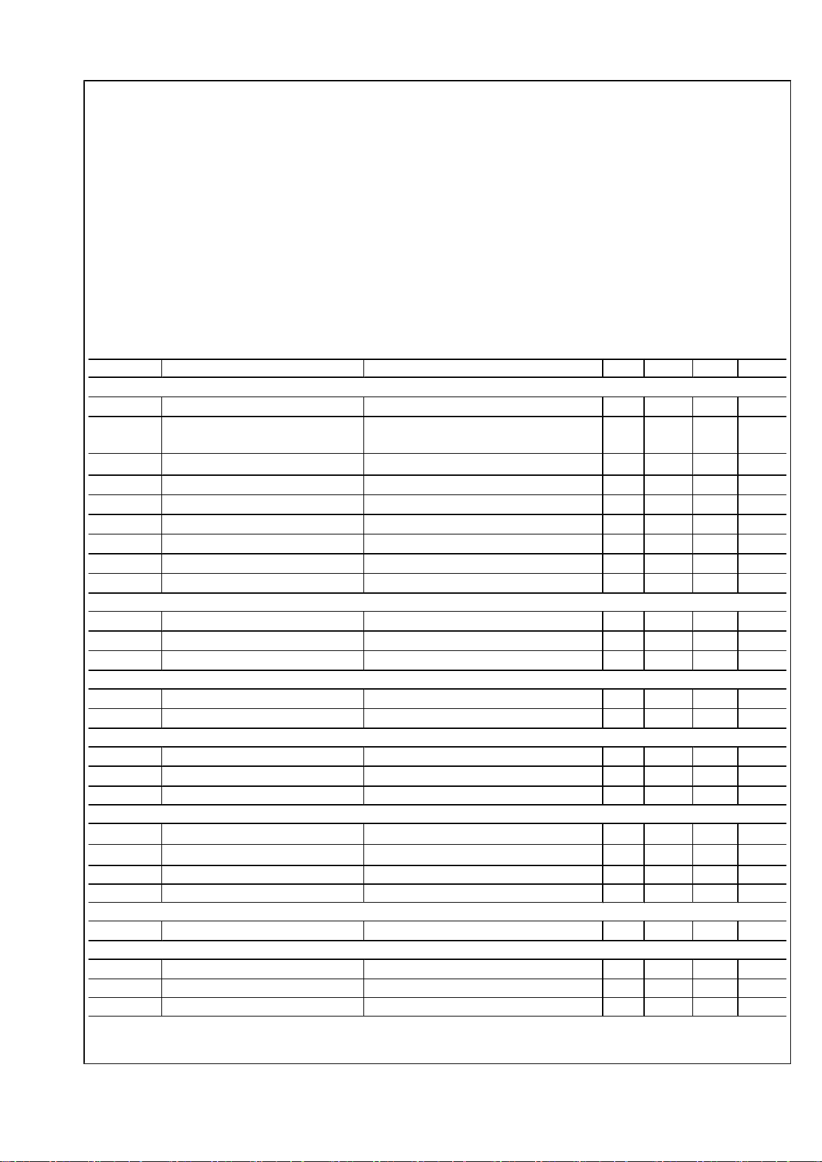
Electrical Characteristics Specifications with standard type are for T
J
= 25°C only; limits in boldface type apply
over the full Operating Junction Temperature (TJ) range. Minimum and Maximum limits are guaranteed through test, design, or
statistical correlation. Typical values represent the most likely parametric norm at TJ = 25°C, and are provided for reference
purposes only. Unless otherwise stated the following conditions apply: VIN = 12V, RON = 200kΩ. See (Note 5).
Symbol Parameter Conditions Min Typ Max Units
Start-Up Regulator, V
CC
VCCReg VCC regulated output 6.6 7 7.4 V
VIN-VCC dropout voltage I
CC
= 0 mA,
VCC = UVLO
VCC
+ 250 mV
1.2 V
VCC output impedance
0 mA ≤ ICC ≤ 5 mA, VIN = 8V
175
Ω
VCC current limit (Note 3) VCC = 0V 9.5 mA
UVLO
VCCVCC
under-voltage lockout threshold VCC increasing 5.7 V
UVLO
VCC
hysteresis VCC decreasing 150 mV
UVLO
VCC
filter delay 100 mV overdrive 3 µs
I
Q
IIN operating current Non-switching, FB = 3V, SW = Open 0.5 0.8 mA
I
SD
IIN shutdown current RON/SD = 0V, SW = Open 75 150 µA
Switch Characteristics
Rds(on) Buck Switch Rds(on) I
TEST
= 200 mA 0.5 1.0
Ω
UVLO
GD
Gate Drive UVLO V
BST
- VSW Increasing 3.0 4.4 5.2 V
UVLOGD hysteresis 480 mV
Softstart Pin
V
SS
Pull-up voltage 2.5 V
Internal current source VSS = 1V 10.5 µA
Current Limit
I
LIM
Threshold Current out of ISEN 0.52 0.64 0.76 A
Resistance from ISEN to SGND 140
mΩ
Response time 150 ns
On Timer
tON - 1 On-time
VIN = 10V, RON = 200 kΩ
2.1 2.77 3.5 µs
tON - 2 On-time
VIN = 40V, RON = 200 kΩ
700 ns
Shutdown threshold Voltage at RON/SD rising 0.45 0.8 1.2 V
Threshold hysteresis Voltage at RON/SD 25 mV
Off Timer
t
OFF
Minimum Off-time 155 ns
Regulation and Over-Voltage Comparators (FB Pin)
V
REF
FB regulation threshold SS pin = steady state 2.440 2.5 2.550 V
FB over-voltage threshold 2.9 V
FB bias current FB = 3V 1 nA
www.national.com 4
LM34919

Symbol Parameter Conditions Min Typ Max Units
Thermal Shutdown
T
SD
Thermal shutdown temperature 175 °C
Thermal shutdown hysteresis 20 °C
Thermal Resistance
θ
JA
Junction to Ambient
0 LFPM Air Flow
61 °C/W
Note 1: Absolute Maximum Ratings are limits beyond which damage to the device may occur. Operating Ratings are conditions under which operation of the
device is intended to be functional. For guaranteed specifications and test conditions, see the Electrical Characteristics.
Note 2: The human body model is a 100pF capacitor discharged through a 1.5kΩ resistor into each pin.
Note 3: VCC provides self bias for the internal gate drive and control circuits. Device thermal limitations limit external loading
Note 4: For detailed information on soldering micro SMD package, refer to the Application Note AN-1112.
Note 5: Typical specifications represent the most likely parametric norm at 25°C operation.
5 www.national.com
LM34919
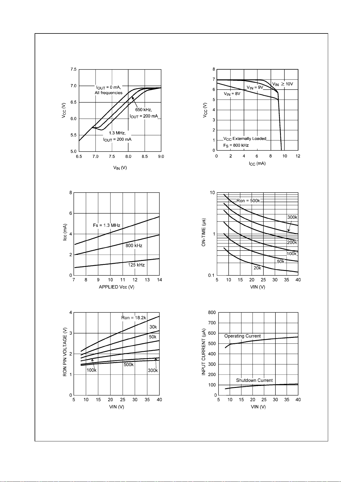
Typical Performance Characteristics
VCC vs V
IN
30004404
VCC vs I
CC
30004405
ICC vs Externally Applied V
CC
30004435
ON-TIME vs VIN and R
ON
30004436
Voltage at the R
ON/SD
Pin
30004437
Shutdown and Operating Current into V
IN
30004438
www.national.com 6
LM34919
 Loading...