

NSC LM348N, LM348MX, LM348MWC, LM348M Datasheet
LM148/LM248/LM348
Quad 741 Op Amps
LM149
Wide Band Decompensated (A
V (MIN)
=
5)
General Description
The LM148 series is a true quad 741. It consists of four independent, high gain, internally compensated, low power operational amplifiers which have been designed to provide
functional characteristics identical to those of the familiar
741 operational amplifier. In addition the total supply current
for all four amplifiers is comparable to the supply current of a
single 741 type op amp. Other features include input offset
currents and input bias current which are much less than
those of a standard 741. Also, excellent isolation between
amplifiers has been achieved by independently biasing each
amplifier and using layout techniques which minimize thermal coupling. The LM149 series has the same features as
the LM148 plus a gain bandwidth product of 4 MHz at a gain
of 5 or greater.
The LM148 can be used anywhere multiple 741or1558type
amplifiers are being used and in applications where amplifier
matching or high packing density is required.
Features
n 741 op amp operating characteristics
n Low supply current drain: 0.6 mA/Amplifier
n Class AB output stage —no crossover distortion
n Pin compatible with the LM124
n Low input offset voltage: 1 mV
n Low input offset current: 4 nA
n Low input bias current: 30 nA
n Gain bandwidth product
LM148 (unity gain): 1.0 MHz
LM149 (A
V
≥ 5): 4 MHz
n High degree of isolation between amplifiers: 120 dB
n Overload protection for inputs and outputs
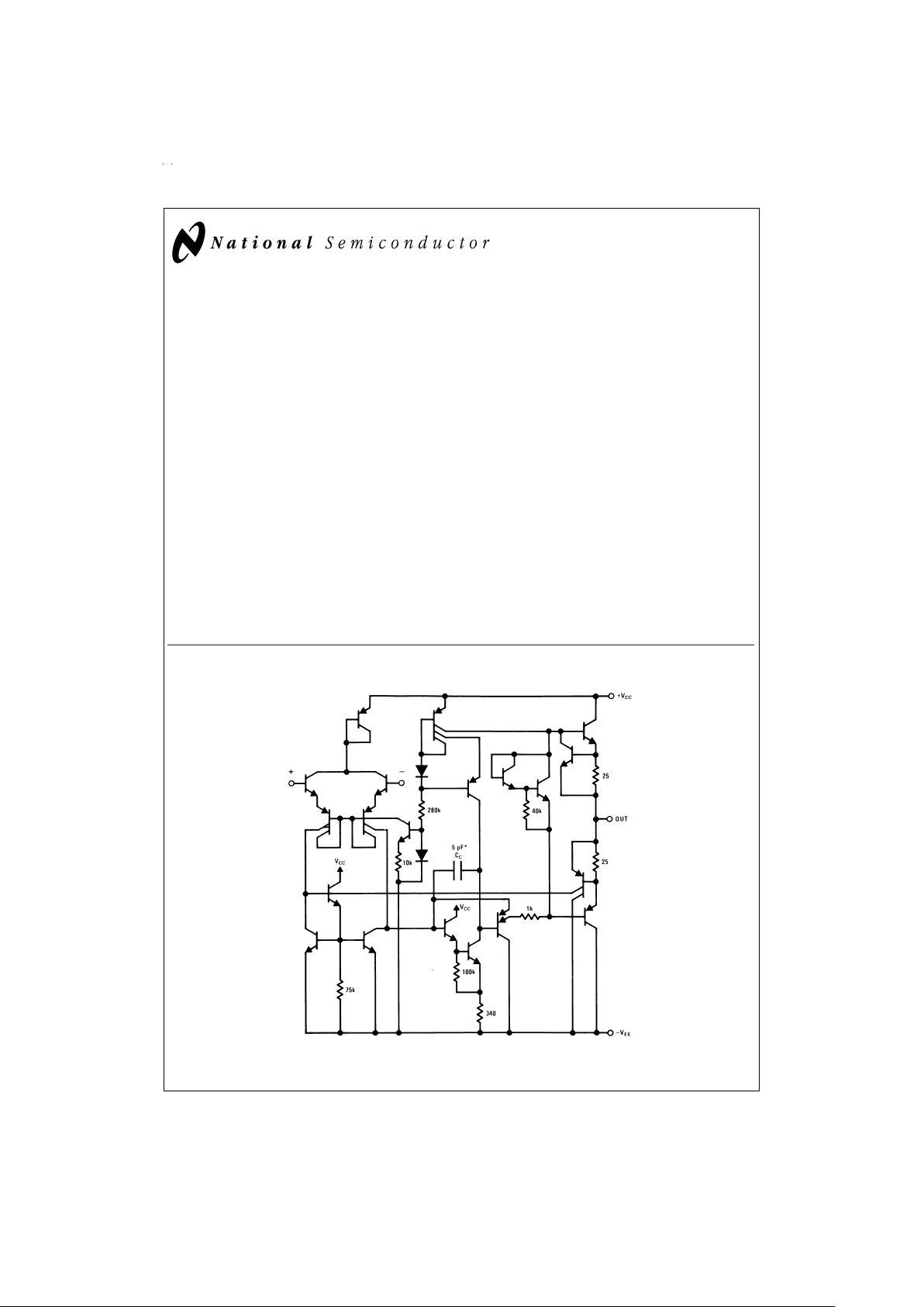
Schematic Diagram
DS007786-1
* 1 pF in the LM149
May 1999
LM148/LM149 Series Quad 741 Op Amp
© 1999 National Semiconductor Corporation DS007786 www.national.com
Absolute Maximum Ratings (Note 4)
If Military/Aerospace specified devices are required, please contact the National Semiconductor Sales Office/
Distributors for availability and specifications.
LM148/LM149 LM248 LM348
Supply Voltage
±
22V
±
18V
±
18V
Differential Input Voltage
±
44V
±
36V
±
36V
Output Short Circuit Duration (Note 1) Continuous Continuous Continuous
Power Dissipation (P
d
at 25˚C) and
Thermal Resistance (θ
jA
), (Note 2)
Molded DIP (N) P
d
— — 750 mW
θ
jA
— — 100˚C/W
Cavity DIP (J) P
d
1100 mW 800 mW 700 mW
θ
JA
110˚C/W 110˚C/W 110˚C/W
Maximum Junction Temperature (T
jMAX
) 150˚C 110˚C 100˚C
Operating Temperature Range −55˚C ≤ T
A
≤ +125˚C −25˚C ≤ TA≤ +85˚C 0˚C ≤ TA≤ +70˚C
Storage Temperature Range −65˚C to +150˚C −65˚C to +150˚C −65˚C to +150˚C
Lead Temperature (Soldering, 10 sec.) Ceramic 300˚C 300˚C 300˚C
Lead Temperature (Soldering, 10 sec.) Plastic 260˚C
Soldering Information
Dual-In-Line Package
Soldering (10 seconds) 260˚C 260˚C 260˚C
Small Outline Package
Vapor Phase (60 seconds) 215˚C 215˚C 215˚C
Infrared (15 seconds) 220˚C 220˚C 220˚C
See AN-450 “Surface Mounting Methods and Their Effect on Product Reliability” for other methods of soldering surface mount
devices.
ESD tolerance (Note 5) 500V 500V 500V
Electrical Characteristics
(Note 3)
Parameter Conditions LM148/LM149 LM248 LM348 Units
Min Typ Max Min Typ Max Min Typ Max
Input Offset Voltage T
A
=
25˚C, R
S
≤ 10 kΩ 1.0 5.0 1.0 6.0 1.0 6.0 mV
Input Offset Current T
A
=
25˚C 4 25 4 50 4 50 nA
Input Bias Current T
A
=
25˚C 30 100 30 200 30 200 nA
Input Resistance T
A
=
25˚C 0.8 2.5 0.8 2.5 0.8 2.5 MΩ
Supply Current All Amplifiers T
A
=
25˚C, V
S
=
±
15V 2.4 3.6 2.4 4.5 2.4 4.5 mA
Large Signal Voltage Gain T
A
=
25˚C, V
S
=
±
15V 50 160 25 160 25 160 V/mV
V
OUT
=
±
10V, RL≥ 2kΩ
Amplifier to Amplifier T
A
=
25˚C, f=1Hzto20kHz
Coupling (Input Referred) See Crosstalk −120 −120 −120 dB
Test Circuit
Small Signal Bandwidth LM148 Series 1.0 1.0 1.0 MHz
T
A
=
25˚C
LM149 Series 4.0 4.0 4.0 MHz
Phase Margin LM148 Series (A
V
=
1) 60 60 60 degrees
T
A
=
25˚C
LM149 Series (A
V
=
5) 60 60 60 degrees
Slew Rate LM148 Series (A
V
=
1) 0.5 0.5 0.5 V/µs
T
A
=
25˚C
LM149 Series (A
V
=
5) 2.0 2.0 2.0 V/µs
Output Short Circuit Current T
A
=
25˚C 25 25 25 mA
Input Offset Voltage R
S
≤ 10 kΩ 6.0 7.5 7.5 mV
Input Offset Current 75 125 100 nA
www.national.com 2
Electrical Characteristics (Continued)
(Note 3)
Parameter Conditions LM148/LM149 LM248 LM348 Units
Min Typ Max Min Typ Max Min Typ Max
Input Bias Current 325 500 400 nA
Large Signal Voltage Gain V
S
=
±
15V, V
OUT
=
±
10V, 25 15 15 V/mV
R
L
>
2kΩ
Output Voltage Swing V
S
=
±
15V, R
L
=
10 kΩ
±12±
13
±12±
13
±12±
13 V
R
L
=
2kΩ
±10±
12
±10±
12
±10±
12 V
Input Voltage Range V
S
=
±
15V
±
12
±
12
±
12 V
Common-Mode Rejection R
S
≤ 10 kΩ 70 90 70 90 70 90 dB
Ratio
Supply Voltage Rejection R
S
≤ 10 kΩ,±5V ≤ VS≤±15V 77 96 77 96 77 96 dB
Note 1: Any of the amplifier outputs can be shortedtoground indefinitely; however, more than one should not be simultaneously shorted as the maximum junction
temperature will be exceeded.
Note 2: Themaximum power dissipation for these devices must be derated at elevated temperatures and is dicated by T
jMAX
, θjA, and the ambient temperature, TA.
The maximum available power dissipation at any temperature is P
d
=
(T
jMAX−TA
)/θjAor the 25˚C P
dMAX
, whichever is less.
Note 3: These specifications apply for V
S
=
±
15V and over the absolute maximum operating temperature range (TL≤ TA≤ TH) unless otherwise noted.
Note 4: Refer to RETS 148X for LM148 military specifications and refer to RETS 149X for LM149 military specifications.
Note 5: Human body model, 1.5 kΩ in series with 100 pF.
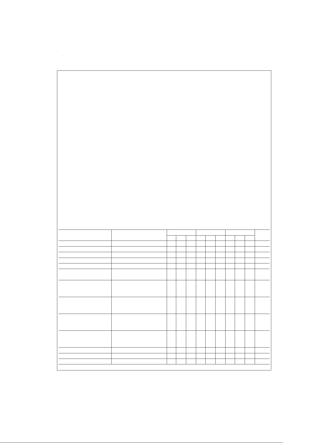
Cross Talk Test Circuit
Application Hints
The LM148 series are quad low power 741 op amps. In the
proliferation of quad op amps, these are the first to offer the
convenience of familiar, easy to use operating characteristics of the 741 op amp. In those applications where 741 op
amps have been employed, the LM148 series op amps can
be employed directly with no change in circuit performance.
The LM149 series has the same characteristics as the
LM148 except it has been decompensated to provide a
wider bandwidth. As a result the part requires a minimum
gain of 5.
The package pin-outs are such that the inverting input of
each amplifier is adjacent to its output. In addition, the amplifier outputs are located in the corners of the package which
simplifies PC board layout and minimizes package related
capacitive coupling between amplifiers.
The input characteristics of these amplifiers allow differential
input voltages which can exceed the supply voltages. In addition, if either of the input voltages is within the operating
common-mode range, the phase of the output remains correct. If the negative limit of the operating common-mode
range is exceeded at both inputs, the output voltage will be
positive. For input voltages which greatly exceed the maximum supply voltages, either differentially or common-mode,
resistors should be placed in series with the inputs to limit
the current.
DS007786-6
DS007786-7
V
S
=
±
15V
www.national.com3
Application Hints (Continued)
Like the LM741, these amplifiers can easily drive a 100 pF
capacitive load throughout the entire dynamic output voltage
and current range. However, if very large capacitive loads
must be driven by a non-inverting unity gain amplifier, a resistor should be placed between the output (and feedback
connection) and the capacitance to reduce the phase shift
resulting from the capacitive loading.
The output current of each amplifier in the package is limited.
Short circuits from an output to either ground or the power
supplies will not destroy the unit. However, if multiple output
shorts occur simultaneously, the time duration should be
short to prevent the unit from being destroyed as a result of
excessive power dissipation in the IC chip.
As with most amplifiers, care should be taken lead dress,
component placement and supply decoupling in order to en-
sure stability.For example, resistors from the output to an input should be placed with the body close to the input to minimize “pickup” and maximize the frequency of the feedback
pole which capacitance from the input to ground creates.
A feedback pole is created when the feedback around any
amplifier is resistive. The parallel resistance and capacitance
from the input of the device (usually the inverting input) toAC
ground set the frequency of the pole. In many instances the
frequency of this pole is much greater than the expected 3
dB frequency of the closed loop gain and consequently there
is negligible effect on stability margin. However, if the feedback pole is less than approximately six times the expected
3 dB frequency a lead capacitor should be placed from the
output to the input of the op amp. The value of the added capacitor should be such that the RC time constant of this capacitor and the resistance it parallels is greater than or equal
to the original feedback pole time constant.
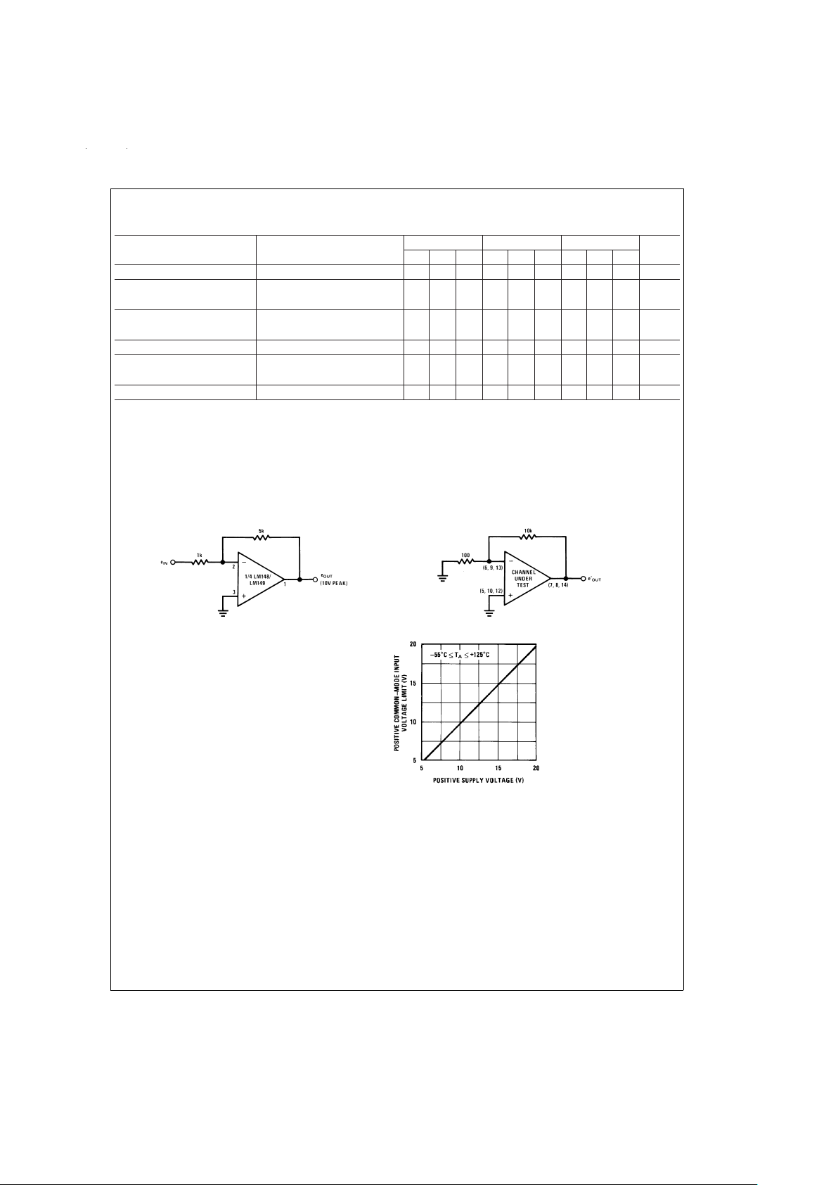
Typical Performance Characteristics
Supply Current
DS007786-23
Input Bias Current
DS007786-24
Voltage Swing
DS007786-25
Positive Current Limit
DS007786-26
Negative Current Limit
DS007786-27
Output Impedance
DS007786-28
www.national.com 4
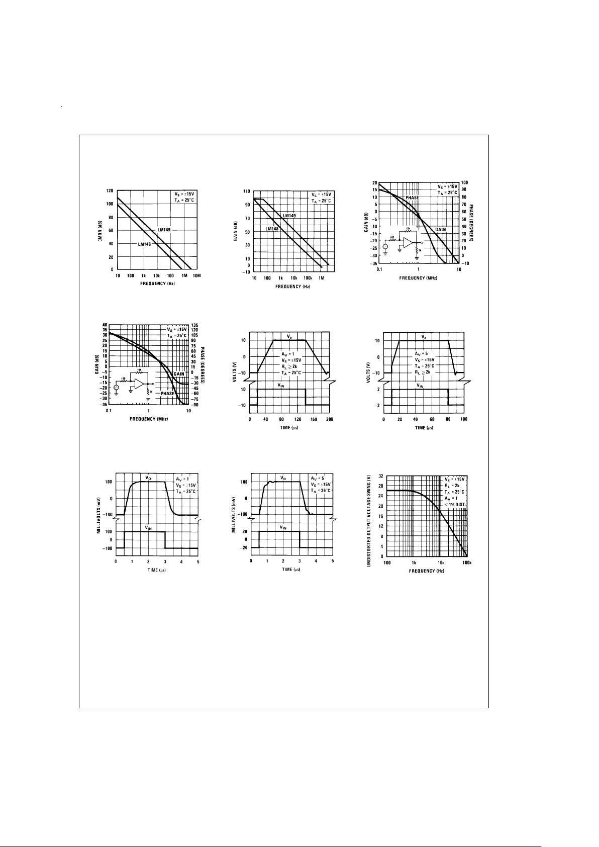
Typical Performance Characteristics (Continued)
Common-Mode Rejection
Ratio
DS007786-29
Open Loop Frequency
Response
DS007786-30
Bode Plot LM148
DS007786-31
Bode Plot LM149
DS007786-32
Large Signal Pulse
Response (LM148)
DS007786-33
Large Signal Pulse
Response (LM149)
DS007786-34
Small Signal Pulse
Response (LM148)
DS007786-35
Small Signal Pulse
Response (LM149)
DS007786-36
Undistorted Output
Voltage Swing
DS007786-37
www.national.com5
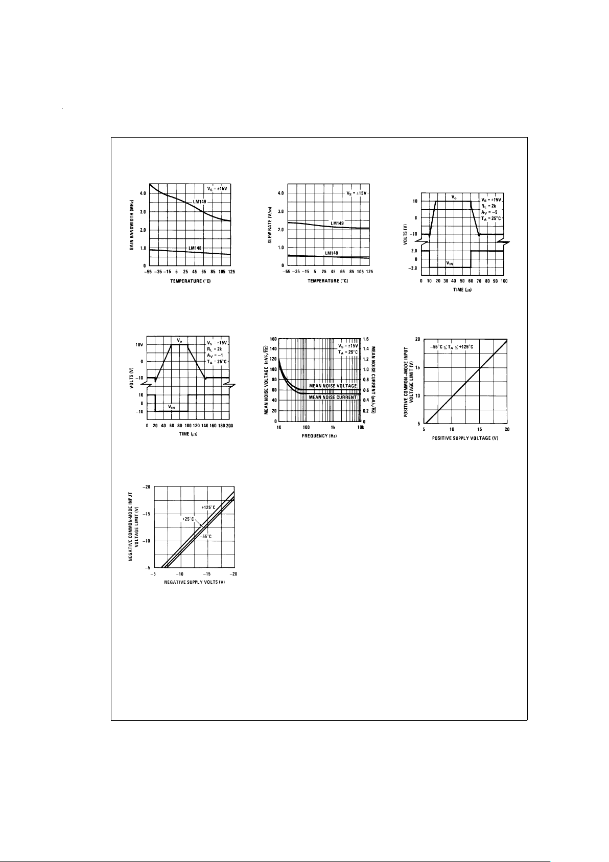
Typical Performance Characteristics (Continued)
Gain Bandwidth
DS007786-38
Slew Rate
DS007786-39
Inverting Large Signal Pulse
Response (LM149)
DS007786-40
Inverting Large Signal Pulse
Response (LM148)
DS007786-41
Input Noise Voltage and
Noise Current
DS007786-42
Positive Common-Mode
Input Voltage Limit
DS007786-43
Negative Common-Mode Input
Voltage Limit
DS007786-5
www.national.com 6
 Loading...