

NSC LM3488MMX, LM3488MM Datasheet
LM3488
High Efficiency Low-Side N-Channel Controller for
Switching Regulators
±
n
General Description
The LM3488 is a versatile Low-Side N-FET high performance controller for switching regulators. It is suitable for
use in topologies requiring low side FET, such as boost,
flyback, SEPIC, etc. Moreover, the LM3488 can be operated
at extremely high switching frequency in order to reduce the
overall solution size. The switching frequency of LM3488 can
be adjusted to any value between 100kHz and 1MHz by
using a single external resistor or by synchronizing it to an
external clock. Current mode control provides superior bandwidth and transient response, besides cycle-by-cycle current
limiting. Output current can be programmed with a single
external resistor.
The LM3488 has built in features such as thermal shutdown,
short-circuit protection and over voltage protection. Power
saving shutdown mode reduces the total supply current to
5µA and allows power supply sequencing. Internal soft-start
limits the inrush current at start-up.
Key Specifications
n Wide supply voltage range of 2.97V to 40V
n 100kHz to 1MHz Adjustable and Synchronizable clock
frequency
1.5% (over temperature) internal reference
n 5µA shutdown current (over temperature)
Features
n 8-lead Mini-SO8 (MSOP-8) package
n Internal push-pull driver with 1A peak current capability
n Current limit and thermal shutdown
n Frequency compensation optimized with a capacitor and
a resistor
n Internal softstart
n Current Mode Operation
n Undervoltage Lockout with hysteresis
Applications
n Distributed Power Systems
n Notebook, PDA, Digital Camera, and other Portable
Applications
n Offline Power Supplies
n Set-Top Boxes
LM3488 High Efficiency Low-Side N-Channel Controller for Switching Regulators
May 2003
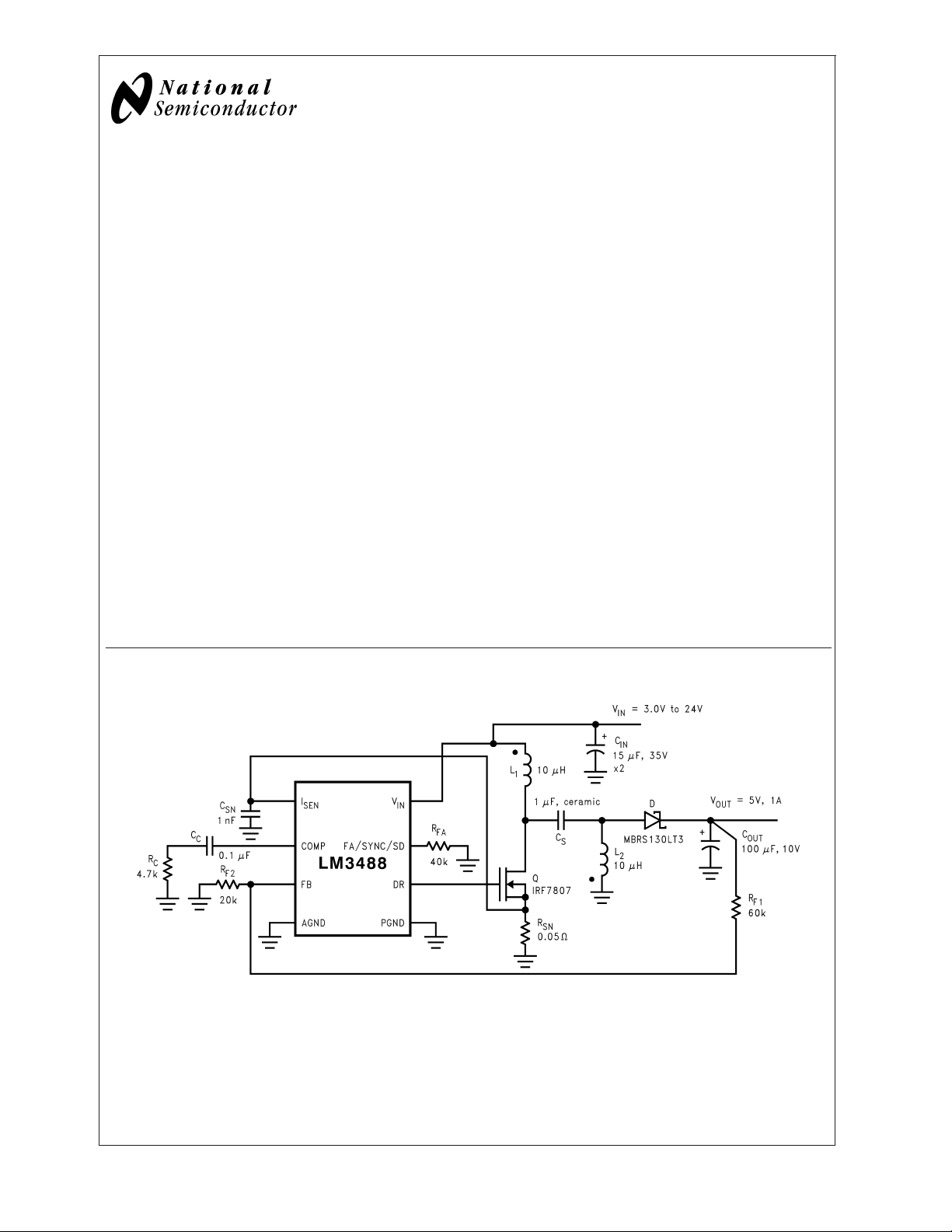
Typical Application Circuit
Typical SEPIC Converter
10138844
© 2003 National Semiconductor Corporation DS101388 www.national.com
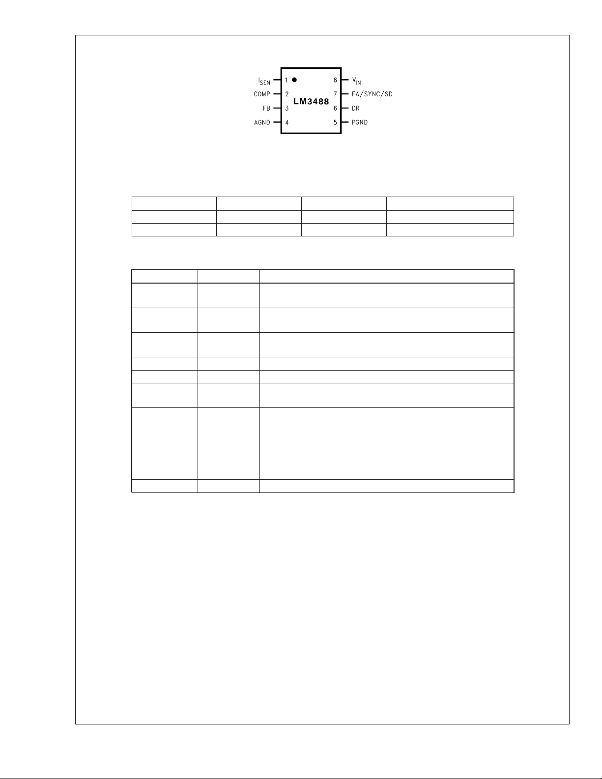
Connection Diagram
LM3488
8 Lead Mini SO8 Package (MSOP-8 Package)
Package Marking and Ordering Information
Order Number Package Type Package Marking Supplied As:
LM3488MM MSOP-8 S21B 1000 units on Tape and Reel
LM3488MMX MSOP-8 S21B 3500 units on Tape and Reel
Pin Description
Pin Name Pin Number Description
I
SEN
COMP 2 Compensation pin. A resistor, capacitor combination connected to
FB 3 Feedback pin. The output voltage should be adjusted using a
AGND 4 Analog ground pin.
PGND 5 Power ground pin.
DR 6 Drive pin of the IC. The gate of the external MOSFET should be
FA/SYNC/SD 7 Frequency adjust, synchronization, and Shutdown pin. A resistor
V
IN
1 Current sense input pin. Voltage generated across an external
sense resistor is fed into this pin.
this pin provides compensation for the control loop.
resistor divider to provide 1.26V at this pin.
connected to this pin.
connected to this pin sets the oscillator frequency. An external
clock signal at this pin will synchronize the controller to the
frequency of the clock. A high level on this pin for ≥ 30µs will turn
the device off. The device will then draw less than 10µA from the
supply.
8 Power supply input pin.
10138802
www.national.com 2
LM3488
Absolute Maximum Ratings (Note 1)
If Military/Aerospace specified devices are required,
please contact the National Semiconductor Sales Office/
Distributors for availability and specifications.
Input Voltage 45V
<
<
FA/SYNC/SD
V
FB
<
FB Pin Voltage -0.4V
FA/SYNC/SD Pin Voltage -0.4V
V
Peak Driver Output Current (
<
10µs) 1.0A
Power Dissipation Internally Limited
Storage Temperature Range −65˚C to +150˚C
Junction Temperature +150˚C
ESD Susceptibilty
7V
<
7V
Lead Temperature
MM Package
Vapor Phase (60 sec.)
Infared (15 sec.)
DR Pin Voltage −0.4V ≤ VDR ≤ 8V
I
Pin Voltage 600mV
LIM
Operating Ratings (Note 1)
Supply Voltage 2.97V ≤ V
Junction
Temperature Range −40˚C ≤ TJ≤ +125˚C
Switching Frequency 100kHz ≤ F
SW
IN
≤ 1MHz
Human Body Model (Note 2) 2kV
Electrical Characteristics
Specifications in Standard type face are for TJ= 25˚C, and in bold type face apply over the full Operating Temperature
Range. Unless otherwise specified, V
Symbol Parameter Conditions Typical Limit Units
V
∆V
FB
LINE
Feedback Voltage V
Feedback Voltage
Line Regulation
∆V
LOAD
Output Voltage Load
Regulation
V
UVLO
Input Undervoltage
Lock-out
V
UV(HYS)
Input Undervoltage
Lock-out Hysteresis
F
nom
Nominal Switching
Frequency
R
DS1 (ON)
Driver Switch On
Resistance (top)
R
DS2 (ON)
Driver Switch On
Resistance (bottom)
V
DR (max)
Maximum Drive
Voltage Swing(Note 6)
D
max
Maximum Duty
Cycle(Note 7)
(on) Minimum On Time 325
T
min
I
SUPPLY
Supply Current
(switching)
I
Q
Quiescent Current in
Shutdown Mode
V
SENSE
Current Sense
Threshold Voltage
= 12V, RFA= 40kΩ
IN
COMP
2.97 ≤ V
= 1.4V,
≤ 40V
IN
1.26
1.2507/1.24
1.2753/1.28
2.97 ≤ VIN≤ 40V 0.001 %/V
I
EAO
Source/Sink
±
0.5 %/V (max)
2.85
2.97
170
130
210
RFA= 40KΩ 400
370
420
IDR= 0.2A, VIN=5V 16 Ω
IDR= 0.2A 4.5 Ω
<
V
7.2V V
IN
V
≥ 7.2V 7.2
IN
IN
100 %
230
550
(Note 9)
V
FA/SYNC/SD
10), V
IN
= 5V(Note
=5V
2.0
5
2.6
7
VIN= 5V 165
140/ 135
195/ 200
V(min)
V(max)
V(max)
mV (min)
mV (max)
kHz
kHz(min)
kHz(max)
nsec
nsec(min)
nsec(max)
mA (max)
µA (max)
mV (min)
mV (max)
215˚C
220˚C
≤ 40V
V
V
mV
V
mA
µA
mV
www.national.com3
Electrical Characteristics (Continued)
Specifications in Standard type face are for TJ= 25˚C, and in bold type face apply over the full Operating Temperature
LM3488
Range. Unless otherwise specified, V
Symbol Parameter Conditions Typical Limit Units
V
SC
Short-Circuit Current
Limit Sense Voltage
V
SL
Internal Compensation
Ramp Voltage
V
OVP
Output Over-voltage
Protection (with
respect to feedback
voltage) (Note 8)
V
OVP(HYS)
Output Over-Voltage
Protection
Hysteresis(Note 8)
Gm Error Ampifier
Transconductance
A
VOL
Error Amplifier Voltage
Gain
I
EAO
Error Amplifier Output
Current (Source/ Sink)
V
EAO
Error Amplifier Output
Voltage Swing
T
SS
Internal Soft-Start
Delay
T
r
T
f
Drive Pin Rise Time Cgs = 3000pf, VDR=0to
Drive Pin Fall Time Cgs = 3000pf, VDR=0to
VSD Shutdown and
Synchronization signal
threshold (Note 5)
I
SD
Shutdown Pin Current VSD=5V −1 µA
TSD Thermal Shutdown 165 ˚C
T
sh
Thermal Shutdown
Hysteresis
θ
JA
Thermal Resistance MM Package 200 ˚C/W
= 12V, RFA= 40kΩ
IN
VIN= 5V 325
VIN=5V 92
= 1.4V 50
V
COMP
= 1.4V 60
V
COMP
= 1.4V
V
COMP
= 100µA
I
EAO
(Source/Sink)
V
= 1.4V
COMP
= 100µA
I
EAO
(Source/Sink)
Source, V
=0V
V
FB
Sink, V
COMP
COMP
= 1.4V, V
= 1.4V,
FB
= 1.4V
Upper Limit
=0V
V
FB
COMP Pin = Floating
Lower Limit
= 1.4V
V
FB
VFB= 1.2V, V
COMP
=
Floating
3V
3V
Output = High 1.27
Output = Low 0.65
V
=0V +1
SD
235
395
52
132
32/ 25
78/ 85
20
110
800
600/ 365
1000/ 1265
38
26
44
110
80/ 50
140/ 180
−140
−100/ −85
−180/ −185
2.2
1.8
2.4
0.56
0.2
1.0
4 msec
25 ns
25 ns
1.35
0.35
10 ˚C
mV
mV (min)
mV (max)
mV
mV(min)
mV(max)
mV
mV(min)
mV(max)
mV
mV(min)
mV(max)
µmho
µmho (min)
µmho (max)
V/V
V/V (min)
V/V (max)
µA
µA (min)
µA (max)
µA
µA (min)
µA (max)
V
V(min)
V(max)
V
V(min)
V(max)
V
V (max)
V
V (min)
www.national.com 4

Electrical Characteristics (Continued)
Note 1: Absolute Maximum Ratings are limits beyond which damage to the device may occur. Operating Ratings are conditions under which operation of the device
is intended to be functional. For guaranteed specifications and test conditions, see the Electrical Characteristics.
Note 2: The human body model is a 100 pF capacitor discharged through a 1.5kΩ resistor into each pin.
Note 3: All limits are guaranteed at room temperature (standard type face) and at temperature extremes (bold type face). All room temperature limits are 100%
tested. All limits at temperature extremes are guaranteed via correlation using standard Statistical Quality Control (SQC) methods. All limits are used to calculate
Average Outgoing Quality Level (AOQL).
Note 4: Typical numbers are at 25˚C and represent the most likely norm.
Note 5: The FA/SYNC/SD pin should be pulled to V
Note 6: The voltage on the drive pin, V
than or equal to 7.2V.
Note 7: The limits for the maximum duty cycle can not be specified since the part does not permit less than 100% maximum duty cycle operation.
Note 8: The over-voltage protection is specified with respect to the feedback voltage. This is because the over-voltage protection tracks the feedback voltage. The
over-voltage thresold can be calculated by adding the feedback voltage, V
Note 9: For this test, the FA/SYNC/SD Pin is pulled to ground using a 40K resistor .
Note 10: For this test, the FA/SYNC/SD Pin is pulled to 5V using a 40K resistor.
is equal to the input voltage when input voltage is less than 7.2V. VDRis equal to 7.2V when the input voltage is greater
DR
through a resistor to turn the regulator off.
IN
to the over-voltage protection specification.
FB
LM3488
www.national.com5
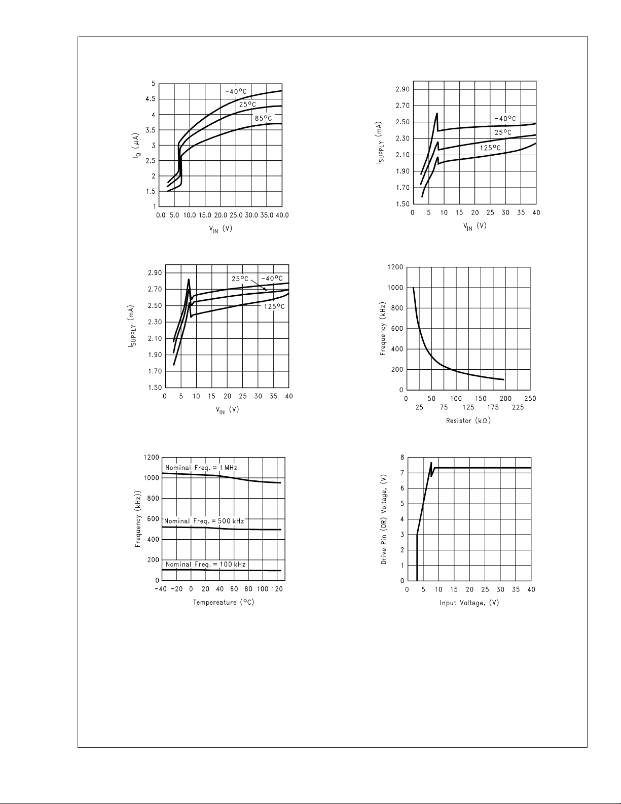
Typical Performance Characteristics Unless otherwise specified, V
LM3488
vs Temperature & Input Voltage I
I
Q
Supply
= 12V, TJ= 25˚C.
IN
vs Input Voltage (Non-Switching)
10138803
I
Supply
vs V
IN
10138835
Switching Frequency vs RFA
Frequency vs Temperature Drive Voltage vs Input Voltage
10138834
10138804
10138854
www.national.com 6
10138805
LM3488
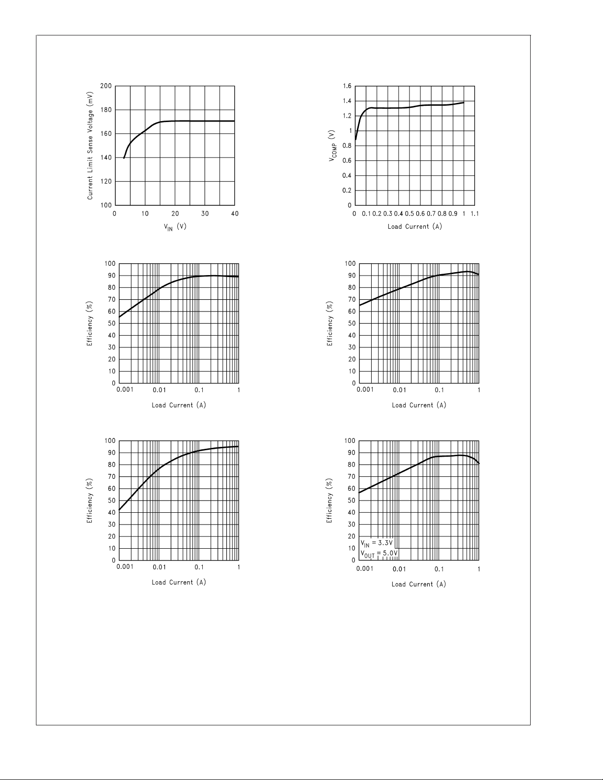
Typical Performance Characteristics Unless otherwise specified, V
= 12V, TJ= 25˚C. (Continued)
IN
Current Sense Threshold vs Input Voltage COMP Pin Voltage vs Load Current
10138845
Efficiency vs Load Current (3.3V In and 12V Out) Efficiency vs Load Current (5V In and 12V Out)
10138862
10138859 10138858
Efficiency vs Load Current (9V In and 12V Out) Efficiency vs Load Current (3.3V In and 5V Out)
10138860
10138853
www.national.com7
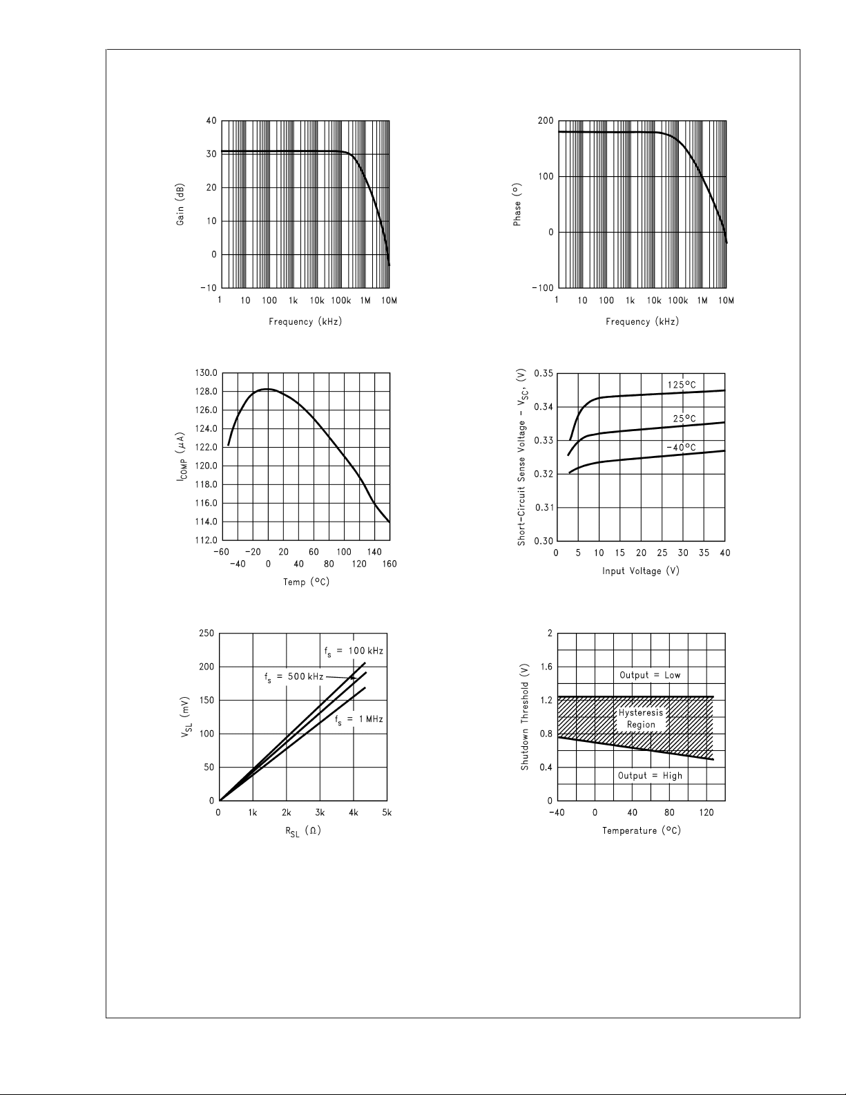
Typical Performance Characteristics Unless otherwise specified, V
LM3488
COMP Pin Source Current vs Temperature Short Circuit Protection vs Input Voltage
Error Amplifier Gain Error Amplifier Phase
10138855 10138856
= 12V, TJ= 25˚C. (Continued)
IN
10138836
10138857
Compensation Ramp vs Compensation Resistor Shutdown Threshold Hysteresis vs Temperature
10138851
10138846
www.national.com 8
 Loading...