

NSC LM3477MMX, LM3477MM, LM3477AMM Datasheet
LM3477/LM3477A
High Efficiency High-Side N-Channel Controller for
Switching Regulator
General Description
The LM3477/A is a high-side N-channel MOSFET switching
regulator controller. It can be used in topologies requiring a
high side MOSFET such as buck, inverting (buck-boost) and
zeta regulators. The LM3477/A’s internal push pull driver
allows compatibility with a wide range of MOSFETs. This, the
wide input voltage range, use of discrete power components
and adjustable current limit allows the LM3477/A to be optimized for a wide variety of applications.
The LM3477/A uses a high switching frequency of 500kHz to
reduce the overall solution size. Current-mode control requires only a single resistor and capacitor for frequency
compensation. The current mode architecture also yields
superior line and load regulation and cycle-by-cycle current
limiting. A 5µA shutdown state can be used for power savings and for power supply sequencing. Other features include internal soft-start and output over voltage protection.
The internal soft-start reduces inrush current. Over voltage
protection is a safety feature to ensure that the output voltage stays within regulation.
The LM3477A is similar to the LM3477. The primary difference between the two is the point at which the device
transitions into hysteretic mode. The hysteretic threshold of
the LM3477A is one-third of the LM3477.
Features
n 500kHz switching frequency
n Adjustable current limit
n 1.5% reference
n Thermal shutdown
n Frequency compensation optimized with a single
capacitor and resistor
n Internal softstart
n Current mode operation
n Undervoltage lockout with hysteresis
n 8-lead Mini-SO8 (MSOP-8) package
Applications
n Local Voltage Regulation
n Distributed Power
n Notebook and Palmtop Computers
n Internet Appliances
n Printers and Office Automation
n Battery operated Devices
n Cable Modems
n Battery Chargers
Hysteretic
Threshold
LM3477 ) 36% of
programmed current
limit
LM3477A ) 12% of
programmed current
limit
*
See Hysteretic Threshold and section for more information.
LM3477/LM3477A High Efficiency High-Side N-Channel Controller for Switching Regulator
June 2002
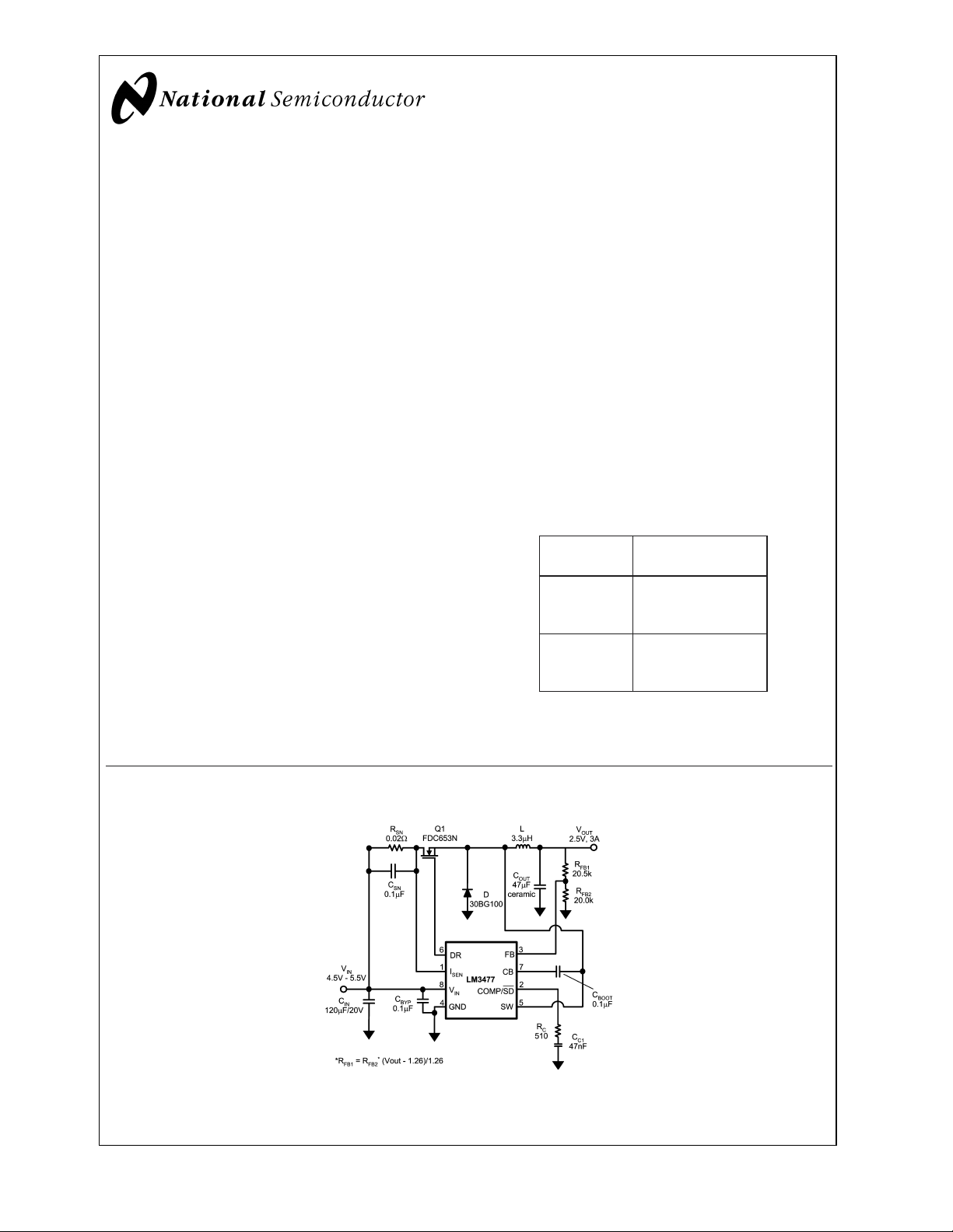
Typical Application Circuit
Typical High Efficiency Step-Down (Buck) Converter
© 2002 National Semiconductor Corporation DS200033 www.national.com
20003333
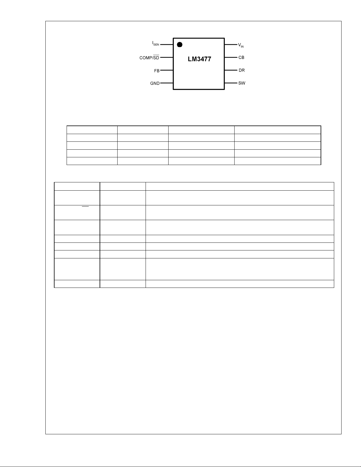
Connection Diagram
LM3477/LM3477A
8 Lead Mini SO8 Package (MSOP-8 Package)
Package Marking and Ordering Information
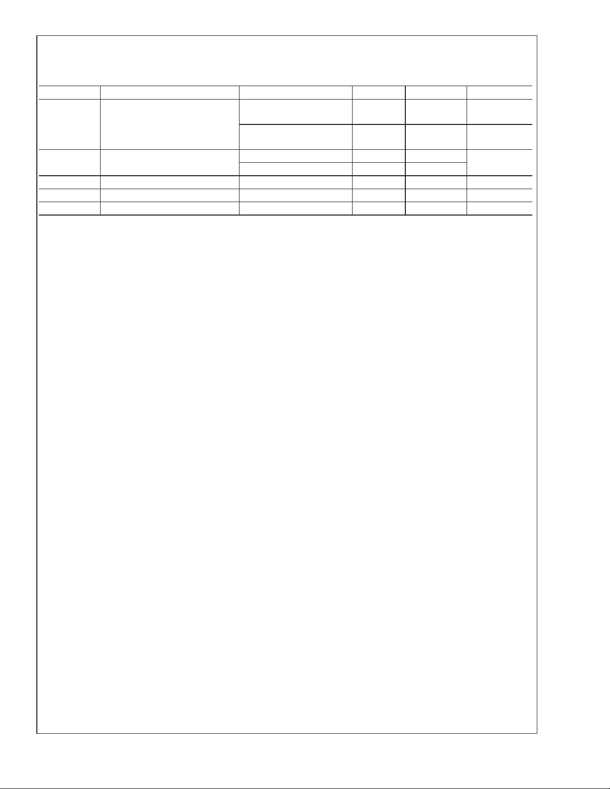
Order Number Package Type Package Marking Supplied As:
LM3477MM MSOP-8 S13B 1000 units on Tape and Reel
LM3477MMX MSOP-8 S13B 3500 units on Tape and Reel
LM3477AMM MSOP-8 S13A 1000 units on Tape and Reel
LM3477AMMX MSOP-8 S13A 3500 units on Tape and Reel
Pin Description
Pin Name Pin Number Description
I
SEN
COMP/SD
FB 3 Feedback pin. The output voltage should be adjusted using a resistor divider to
GND 4 Ground pin.
SW 5 Switch Node. Source of the external MOSFET is connected to this node.
DR 6 Drive pin. The gate of the external MOSFET should be connected to this pin.
CB 7 Boot-strap pin. A capacitor must be connected between this pin and SW pin (pin 5)
V
IN
1 Current sense input pin. Voltage generated across an external sense resistor is fed
into this pin.
2 Compensation pin. A resistor-capacitor combination connected to this pin provides
compensation for the control loop. Pull this pin below 0.65V to shutdown.
provide 1.270V at this pin.
for proper operation. The voltage developed across this capacitor provides the gate
drive for the external MOSFET.
8 Power Supply Input pin.
20003302
www.national.com 2
LM3477/LM3477A
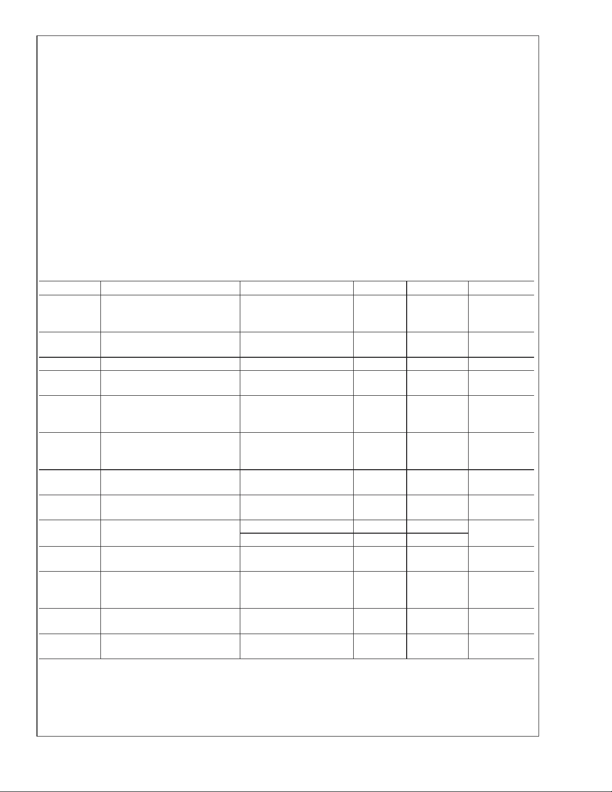
Absolute Maximum Ratings (Note 1)
If Military/Aerospace specified devices are required,
please contact the National Semiconductor Sales Office/
Lead Temperature for MSOP Package
Vapor Phase (60 sec.)
Infared (15 sec.)
Distributors for availability and specifications.
Input Voltage 36V
<
Peak Driver Output Current (
10µs) 1.0A
CB Pin Voltage (Note 2) 43V
I
Pin Voltage 500mV
SEN
Power Dissipation Internally Limited
Operating Ratings (Note 1)
Supply Voltage 2.97V ≤ V
Junction
Temperature Range −40˚C ≤ T
IN
≤ +125˚C
J
Storage Temperature Range −65˚C to +150˚C
Junction Temperature +150˚C
ESD Susceptibilty (Note 3)
Human Body Model
Machine Model
2kV
200V
Electrical Characteristics (Note 4)
Specifications in Standard type face are for TJ= 25˚C, and in bold type face apply over the full Operating Temperature
Range. Unless otherwise specified, V
Symbol Parameter Conditions Typical Limit Units
V
∆V
FB
LINE
Feedback Voltage V
Feedback Voltage Line
Regulation
∆V
V
UVLO
V
UV(HYS)
LOAD
Output Voltage Load Regulation
Input Undervoltage Lock-out 2.87
Input Undervoltage Lock-out
Hysteresis
F
SW
R
DS1 (ON)
Switching Frequency 500
Driver Switch On Resistance
(top)
R
DS2 (ON)
Driver Switch On Resistance
(bottom)
(V
CB−VSW)max
D
max
(on) Minimum On Time 330
T
min
I
SUPPLY
I
Q
Maximum Boot Voltage V
Maximum Duty Cycle 93
Supply Current (switching) (Note 5) 2.0
Quiescent Current in Shutdown
Mode
IN
= 12V.
= 1.4V,
COMP
2.97V ≤ V
IN
≤ 36V
1.270
1.260/1.252
1.288/1.290
V(min)
V(max)
2.97V ≤ VIN≤ 36V 0.001 %/V
±
0.5 %/V (max)
2.97
V(max)
180
130
225
435
575
mV (min)
mV (max)
kHz(min)
kHz(max)
IDR= 0.2A, VIN=5V 7 Ω
IDR= 0.2A 4 Ω
<
7.2V V
IN
V
≥ 7.2V 7.2
IN
IN
88
230
495
3.0
%(min)
nsec(min)
nsec(max)
mA (max)
(Note 6), VIN=5V 5
8
µA (max)
215˚C
220˚C
≤ 35V
V
V
mV
kHz
V
%
nsec
mA
µA
www.national.com3
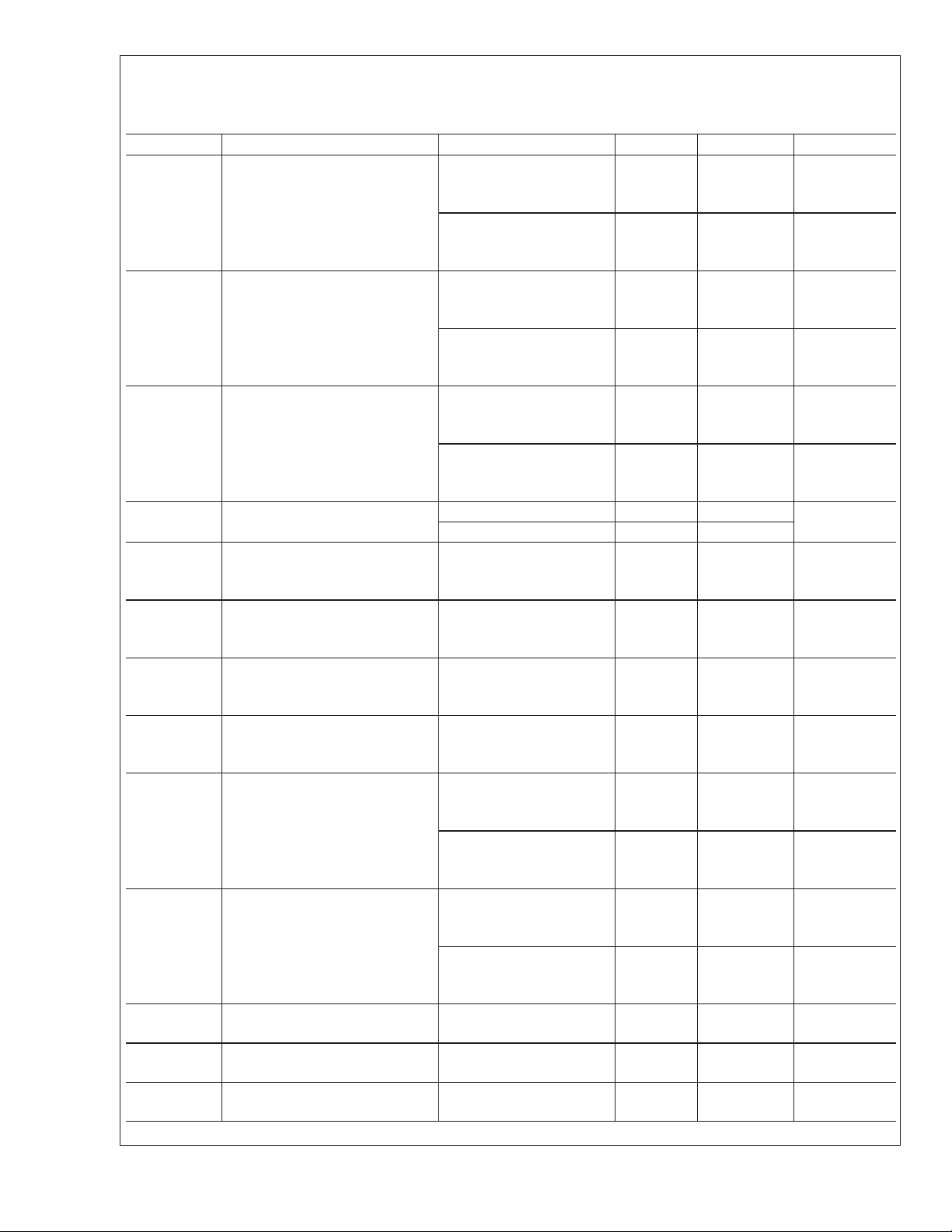
Electrical Characteristics (Note 4) (Continued)
Specifications in Standard type face are for TJ= 25˚C, and in bold type face apply over the full Operating Temperature
Range. Unless otherwise specified, V
Symbol Parameter Conditions Typical Limit Units
V
CL(O)
LM3477/LM3477A
V
CL(100)
Current Limit Voltage at 0% Duty
Cycle
Current Limit Voltage at 100%
Duty Cycle
V
SC
Short-Circuit Current Limit Sense
Voltage
V
SL
Internal Compensation Ramp
Voltage Height
V
OVP
Output Over-voltage Protection
(with respect to feedback
voltage) (Note 7)
V
OVP(HYS)
Output Over-Voltage Protection
Hysteresis(Note 7)
Gm Error Amplifier
Transconductance
A
I
VOL
EAO
Error Amplifier Voltage Gain V
Error Amplifier Output Current
(Source/ Sink)
V
EAO
Error Amplifier Output Voltage
Swing
T
SS
T
r
T
f
Internal Soft-Start Delay VFB= 1.2V, V
Drive Pin Rise Time CGS= 3000pF, VDR=0
Drive Pin Fall Time CGS= 3000pF, VDR=0
IN
= 12V.
LM3477 155
130/125
185/190
LM3477A 165
140/135
195/200
LM3477 74
50/43
98/98
LM3477A 65
41/25
89/98
VIN= 5V, LM3477 350
270
420
= 5V, LM3477A 310
V
IN
260
380
VIN= 5V, LM3477 83 mV
V
= 5V, LM3477A 103
IN
= 1.4V 50
V
COMP
32/25
78/85
V
= 1.4V 60
COMP
20
110
= 1.4V
V
COMP
= 100µA
I
EAO
(Source/Sink)
= 1.4V
COMP
= 100µA
I
EAO
(Source/Sink)
Source, V
V
FB
COMP
=0V
= 1.4V,
750
600/365
1000/1265
38
30
42
100
75/50
130/160
Sink, V
= 1.4V
COMP
= 1.4V, V
FB
−140
−110/−95
−170/−180
Upper Limit
=0V
V
FB
COMP Pin = Floating
Lower Limit
= 1.4V
V
FB
2.2
2.0
2.35
0.75
0.5
0.95
COMP
=
5 msec
Floating
25 ns
to 3V
25 ns
to 3V
mV
mV (min)
mV (max)
mV
mV (min)
mV (max)
mV
mV (min)
mV (max)
mV
mV (min)
mV (max)
mV
mV (min)
mV (max)
mV
mV (min)
mV (max)
mV
mV(min)
mV(max)
mV
mV(min)
mV(max)
µmho
µmho (min)
µmho (max)
V/V
V/V (min)
V/V (max)
µA
µA (min)
µA (max)
µA
µA (min)
µA (max)
V
V(min)
V(max)
V
V(min)
V(max)
www.national.com 4
Electrical Characteristics (Note 4) (Continued)
Specifications in Standard type face are for TJ= 25˚C, and in bold type face apply over the full Operating Temperature
Range. Unless otherwise specified, V
Symbol Parameter Conditions Typical Limit Units
V
SD
I
SD
Shutdown Threshold (Note 8) Output = High 1.15
Shutdown Pin Current VSD=5V −1
TSD Thermal Shutdown 165 ˚C
T
SH
θ
JA
Thermal Shutdown Hysteresis 10 ˚C
Thermal Resistance MM Package 200 ˚C/W
IN
= 12V.
Output = Low 0.65
V
=0V +1
SD
1.35
0.3
V (max)
V (min)
µA
LM3477/LM3477A
V
V
www.national.com5

Electrical Characteristics (Note 4) (Continued)
Note 1: Absolute Maximum Ratings are limits beyond which damage to the device may occur. Operating Ratings are conditions under which operation of the device
is intended to be functional. For guaranteed specifications and test conditions, see the Electrical Characteristics.
Note 2: The CB pin must not be higher than 8V above the V
Note 3: The human body model is a 100 pF capacitor discharged through a 1.5kΩ resistor into each pin. The machine model is 200 pF capacitor discharged directly
into each pin.
Note 4: All limits are guaranteed at room temperature (standard type face) and at temperature extremes (bold type face). All room temperature limits are 100%
LM3477/LM3477A
tested. All limits at temperature extremes are guaranteed via correlation using standard Statistical Quality Control (SQC) methods. All limits are used to calculate
Average Outgoing Quality Level (AOQL).
Note 5: For this test, the COMP/SD pin must be left floating.
Note 6: For this test, the COMP/SD pin must be pulled low.
Note 7: The over-voltage protection is specified with respect to the feedback voltage. This is because the over-voltage protection tracks the feedback voltage. The
overvoltage protection threshold is given by adding the feedback voltage, V
Note 8: The COMP/SD pin should be pulled to ground to turn the regulator off. The voltage on the COMP/SD pin must be below the limit for Output = Low to keep
the regulator off.
SW
.
to the over-voltage protection specification.
FB
www.national.com 6
LM3477/LM3477A
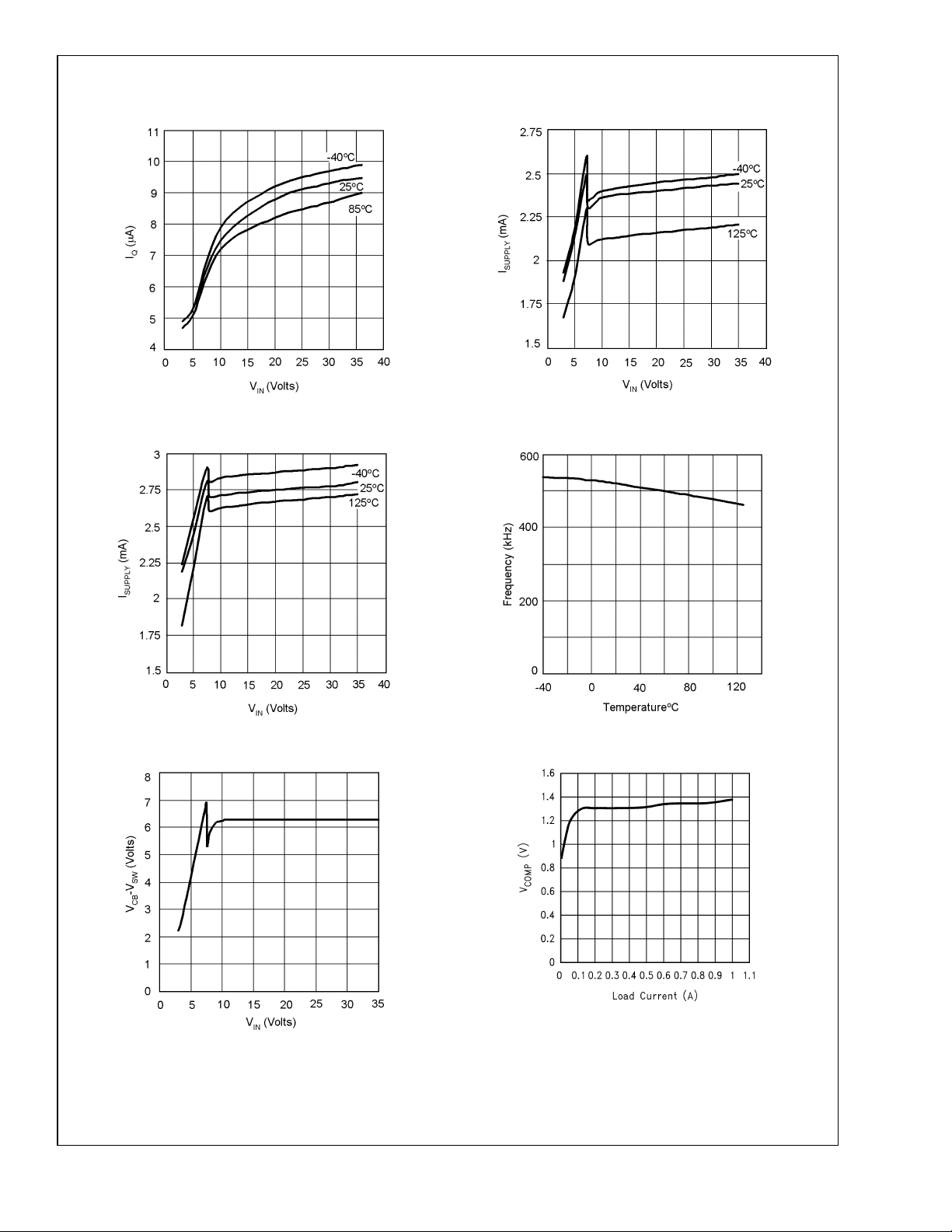
Typical Performance Characteristics Unless otherwise specified, V
(Shutdown) vs Temperature & Supply Voltage I
I
Q
20003313 20003314
I
vs Temperature & Supply Voltage (Switching) Frequency vs Temperature
Supply
vs Temperature & Supply Voltage (Non-Switching)
Supply
= 12V, TJ= 25˚C.
IN
20003315 20003316
VCB−VSWvs Supply Voltage COMP Pin Voltage vs Load Current
20003362
20003320
www.national.com7
 Loading...