


LM317L
3-Terminal Adjustable Regulator
General Description
The LM317L is an adjustable 3-terminal positive voltage
regulator capable of supplying 100mA over a 1.2V to 37V
output range. It is exceptionally easy to use and requires
only two external resistors to set the output voltage. Further,
both line and load regulation are better than standard fixed
regulators.Also, the LM317L is available packaged in a standard TO-92 transistor package which is easy to use.
In addition to higher performance than fixed regulators, the
LM317L offers full overload protection. Included on the chip
are current limit, thermal overload protection and safe area
protection.All overload protection circuitry remains fully functional even if the adjustment terminal is disconnected.
Normally,no capacitors are needed unless the device is situated more than 6 inches from the input filter capacitors in
which case an input bypass is needed. An optional output
capacitor can be added to improve transient response. The
adjustment terminal can be bypassed to achieve very high
ripple rejection ratios which are difficult to achieve with standard 3-terminal regulators.
Besides replacing fixed regulators, the LM317L is useful in a
wide variety of other applications. Since the regulator is
“floating” and sees only the input-to-output differential voltage, supplies of several hundred volts can be regulated as
long as the maximum input-to-output differential is not exceeded.
Also, it makes an especially simple adjustable switching
regulator,a programmable output regulator, or by connecting
a fixed resistor between the adjustment and output, the
LM317L can be used as a precision current regulator. Supplies with electronic shutdown can be achieved by clamping
the adjustment terminal to ground which programs the output to 1.2V where most loads draw little current.
The LM317L is available in a standard TO-92 transistor
package, the SO-8 package, and 6-Bump micro SMD package. The LM317L is rated for operation over a −25˚C to
125˚C range.
Features
n Adjustable output down to 1.2V
n Guaranteed 100 mA output current
n Line regulation typically 0.01%V
n Load regulation typically 0.1%
n Current limit constant with temperature
n Eliminates the need to stock many voltages
n Standard 3-lead transistor package
n 80 dB ripple rejection
n Available in TO-92, SO-8, or 6-Bump micro SMD
package
n Output is short circuit protected
n See AN-1112 for micro SMD considerations
Connection Diagrams
TO-92 Plastic package
DS009064-4
8-Pin SOIC
DS009064-5
Top View
March 2000
LM317L 3-Terminal Adjustable Regulator
© 2000 National Semiconductor Corporation DS009064 www.national.com
Connection Diagrams (Continued)
Package Part Number Package Marking Media Transport NSC Drawing
TO-92 LM317LZ LM317LZ 1.8k Units per Box Z03A
8-Pin SOIC LM317LM LM317LM Rails M08A
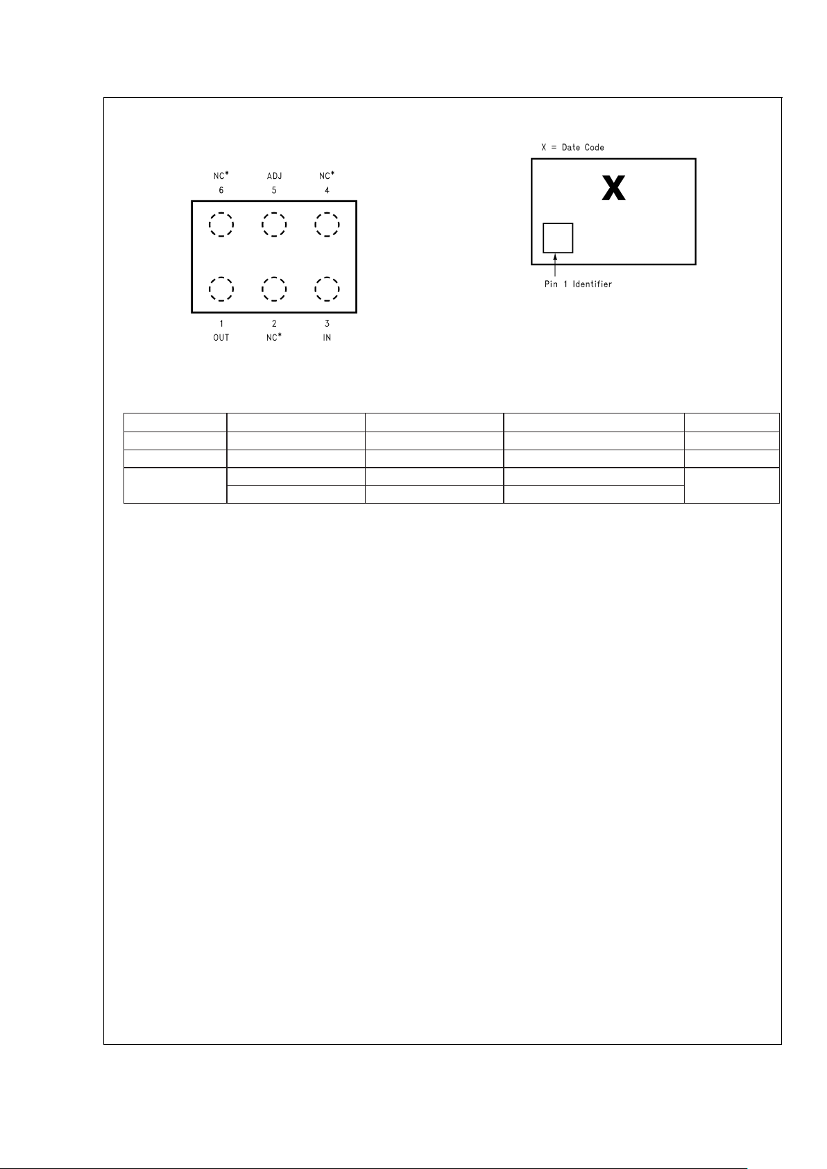
6-Bump micro
SMD
*
LM317LIBP – 250 Units Tape and Reel
BPA06HPA
*
LM317LIBPX – 3k Units Tape and Reel
Note: The micro SMD package marking is a single digit manufacturing Date Code only.
6-Bump micro SMD
DS009064-49
*
NC = Not Internally connected.
Top View
(Bump Side Down)
micro SMD Laser Mark
DS009064-50
LM317L
www.national.com 2
Absolute Maximum Ratings (Note 1)
If Military/Aerospace specified devices are required,
please contact the National Semiconductor Sales Office/
Distributors for availability and specifications.
Power Dissipation Internally Limited
Input-Output Voltage Differential 40V
Operating Junction Temperature
Range −40˚C to +125˚C
Storage Temperature −55˚C to +150˚C
Lead Temperature
(Soldering, 4 seconds) 260˚C
Output is Short Circuit Protected
ESD rating to be determined.
Electrical Characteristics (Note 2)
Parameter Conditions Min Typ Max Units
Line Regulation T
J
= 25˚C, 3V ≤ (VIN−V
OUT
) ≤ 40V, IL≤ 20mA (Note 3) 0.01 0.04 %/V
Load Regulation T
J
= 25˚C, 5mA ≤ I
OUT
≤ I
MAX
, (Note 3) 0.1 0.5 %
Thermal Regulation T
J
= 25˚C, 10ms Pulse 0.04 0.2 %/W
Adjustment Pin Current 50 100 µA
Adjustment Pin Current 5mA ≤ I
L
≤ 100mA 0.2 5 µA
Change 3V ≤ (V
IN−VOUT
) ≤ 40V, P ≤ 625mW
Reference Voltage 3V ≤ (V
IN−VOUT
) ≤ 40V, (Note 4) 1.20 1.25 1.30 V
5mA ≤ I
OUT
≤ 100mA, P ≤ 625mW
Line Regulation 3V ≤ (V
IN−VOUT
) ≤ 40V, IL≤ 20mA (Note 3) 0.02 0.07 %/V
Load Regulation 5mA ≤ I
OUT
≤ 100mA, (Note 3) 0.3 1.5 %
Temperature Stability T
MIN
≤ TJ≤ T
Max
0.65 %
Minimum Load Current (V
IN−VOUT
) ≤ 40V 3.5 5 mA
3V ≤ (V
IN−VOUT
) ≤ 15V 1.5 2.5
Current Limit 3V ≤ (V
IN−VOUT
) ≤ 13V 100 200 300 mA
(V
IN−VOUT
) = 40V 25 50 150 mA
Rms Output Noise, % of V
OUT
TJ= 25˚C, 10Hz ≤ f ≤ 10kHz 0.003 %
Ripple Rejection Ratio V
OUT
= 10V, f = 120Hz, C
ADJ
= 0 65 dB
C
ADJ
= 10µF 66 80 dB
Long-Term Stability T
J
= 125˚C, 1000 Hours 0.3 1 %
Thermal Resistance Z Package 0.4" Leads 180 ˚C/W
Junction to Ambient Z Package 0.125 Leads 160 ˚C/W
SO-8 Package 165 ˚C/W
6-Bump micro SMD 290 ˚C/W
Thermal Rating of SO
Package
165 ˚C/W
Note 1: “Absolute Maximum Ratings” indicate limits beyond which damage to the device may occur. Operating Ratings indicate conditions for which the device is
functional, but do not guarantee specific performance limits.
Note 2: Unless otherwise noted, these specifications apply: −25˚C ≤ T
j
≤ 125˚C for the LM317L; VIN−V
OUT
= 5V and I
OUT
= 40 mA. Although power dissipation
is internally limited, these specifications are applicable for power dissipations up to 625 mW. I
MAX
is 100 mA.
Note 3: Regulation is measured at constant junction temperature, using pulse testing with a low duty cycle. Changes in output voltage due to heating effects are covered under the specification for thermal regulation.
Note 4: Thermal resistance of the TO-92 package is 180˚C/W junction to ambient with 0.4" leads from a PC board and 160˚C/W junction to ambient with 0.125" lead
length to PC board.
LM317L
www.national.com3
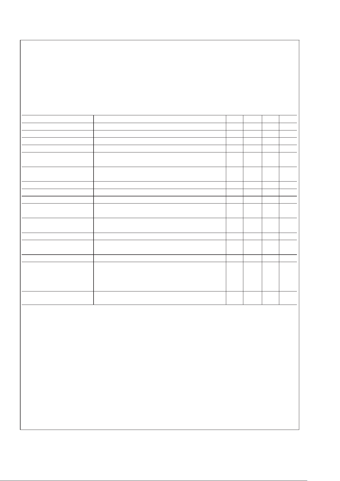
Typical Performance Characteristics (Output capacitor = 0µF unless otherwise noted.)
Load Regulation
DS009064-34
Current Limit
DS009064-35
Adjustment Current
DS009064-36
Dropout Voltage
DS009064-37
Reference Voltage
Temperature Stability
DS009064-38
Minimum Operating Current
DS009064-39
LM317L
www.national.com 4
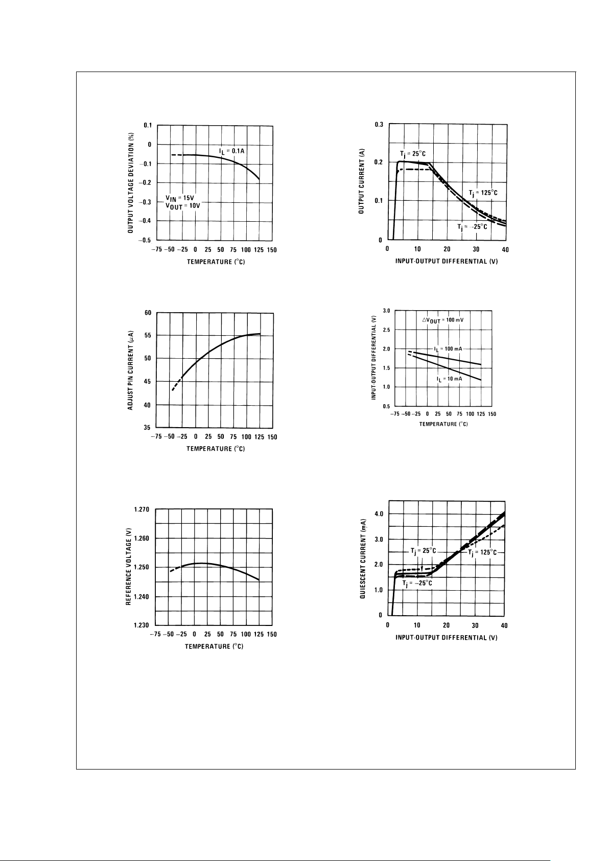
Typical Performance Characteristics (Output capacitor = 0µF unless otherwise noted.) (Continued)
Ripple Rejection
DS009064-40
Ripple Rejection
DS009064-41
Output Impedance
DS009064-42
Line Transient Response
DS009064-43
Load Transient Response
DS009064-44
Thermal Regulation
DS009064-45
LM317L
www.national.com5

Application Hints
In operation, the LM317L develops a nominal 1.25V reference voltage, V
REF
, between the output and adjustment terminal. The reference voltage is impressed across program
resistor R1 and, since the voltage is constant, a constant
current I
1
then flows through the output set resistor R2, giv-
ing an output voltage of
Since the 100µA current from the adjustment terminal represents an error term, the LM317L was designed to minimize
I
ADJ
and make it very constant with line and load changes.
To do this, all quiescent operating current is returned to the
output establishing a minimum load current requirement. If
there is insufficient load on the output, the output will rise.
External Capacitors
An input bypass capacitor is recommended in case the regulator is more than 6 inches away from the usual large filter
capacitor.A 0.1µF disc or 1µF solid tantalum on the input is
suitable input bypassing for almost all applications. The device is more sensitive to the absence of input bypassing
when adjustment or output capacitors are used, but the
above values will eliminate the possibility of problems.
The adjustment terminal can be bypassed to ground on the
LM317L to improve ripple rejection and noise. This bypass
capacitor prevents ripple and noise from being amplified as
the output voltage is increased. With a 10µF bypass capacitor 80 dB ripple rejection is obtainable at any output level. Increases over 10µF do not appreciably improve the ripple rejection at frequencies above 120Hz. If the bypass capacitor
is used, it is sometimes necessary to include protection diodes to prevent the capacitor from discharging through internal low current paths and damaging the device.
In general, the best type of capacitors to use is solid tantalum.
Solid tantalum capacitors have low impedance even at
high frequencies.
Depending upon capacitor construction, it
takes about 25µF in aluminum electrolytic to equal 1µF solid
tantalum at high frequencies. Ceramic capacitors are also
good at high frequencies; but some types have a large decrease in capacitance at frequencies around 0.5MHz. For
this reason, a 0.01µF disc may seem to work better than a
0.1µF disc as a bypass.
Although the LM317L is stable with no output capacitors, like
any feedback circuit, certain values of external capacitance
can cause excessive ringing. This occurs with values be-
tween 500 pF and 5000 pF. A 1µF solid tantalum (or 25µF
aluminum electrolytic) on the output swamps this effect and
insures stability.
Load Regulation
The LM317L is capable of providing extremely good load
regulation but a few precautions are needed to obtain maximum performance. The current set resistor connected between the adjustment terminal and the output terminal (usually 240Ω) should be tied directly to the output of the
regulator rather than near the load. This eliminates line
drops from appearing effectively in series with the reference
and degrading regulation. For example, a 15V regulator with
0.05Ω resistance between the regulator and load will have a
load regulation due to line resistance of 0.05Ω xI
L
. If the set
resistor is connected near the load the effective line resistance will be 0.05Ω (1 + R2/R1) or in this case, 11.5 times
worse.
Figure 2
shows the effect of resistance between the regula-
tor and 240Ω set resistor.
With the TO-92 package, it is easy to minimize the resis-
tance from the case to the set resistor,by using two separate
leads to the output pin. The ground of R2 can be returned
near the ground of the load to provide remote ground sensing and improve load regulation.
Thermal Regulation
When power is dissipated in an IC, a temperature gradient
occurs across the IC chip affecting the individual IC circuit
components. With an IC regulator, this gradient can be especially severe since power dissipation is large. Thermal regulation is the effect of these temperature gradients on output
voltage (in percentage output change) per watt of power
change in a specified time. Thermal regulation error is independent of electrical regulation or temperature coefficient,
and occurs within 5ms to 50ms after a change in power dissipation. Thermal regulation depends on IC layout as well as
electrical design. The thermal regulation of a voltage regulator is defined as the percentage change of V
OUT
, per watt,
within the first 10ms after a step of power is applied. The
LM317L specification is 0.2%/W, maximum.
In the Thermal Regulation curve at the bottom of the Typical
Performance Characteristics page, a typical LM317L’s output changes only 7mV (or 0.07% of V
OUT
= −10V) when a
1W pulse is applied for 10 ms. This performance is thus well
inside the specification limit of 0.2%/W x 1W = 0.2% maximum. When the 1W pulse is ended, the thermal regulation
again showsa7mVchange as the gradients across the
LM317L chip die out. Note that the load regulation error of
about 14 mV (0.14%) is additional to the thermal regulation
error.
DS009064-7
FIGURE 1.
DS009064-8
FIGURE 2. Regulator with Line Resistance
in Output Lead
LM317L
www.national.com 6

Application Hints (Continued)
Protection Diodes
When external capacitors are used with
any
IC regulator it is
sometimes necessary to add protection diodes to prevent
the capacitors from discharging through low current points
into the regulator. Most 10µF capacitors have low enough internal series resistance to deliver 20A spikes when shorted.
Although the surge is short, there is enough energy to damage parts of the IC.
When an output capacitor is connected to a regulator and
the input is shorted, the output capacitor will discharge into
the output of the regulator. The discharge current depends
on the value of the capacitor, the output voltage of the regulator,and the rate of decrease of V
IN
. In the LM317L, this dis-
charge path is through a large junction that is able to sustain
a 2Asurge with no problem. This is not true of other types of
positive regulators. For output capacitors of 25 µF or less,
the LM317L’s ballast resistors and output structure limit the
peak current to a low enough level so that there is no need
to use a protection diode.
The bypass capacitor on the adjustment terminal can discharge through a low current junction. Discharge occurs
when
either
the input or output is shorted. Internal to the
LM317L is a 50Ω resistor which limits the peak discharge
current. No protection is needed for output voltages of 25V
or less and 10µF capacitance.
Figure 3
shows an LM317L
with protection diodes included for use with outputs greater
than 25V and high values of output capacitance.
LM317L micro SMD Light Sensitivity
Exposing the LM317L micro SMD package to bright sunlight
may cause the V
REF
to drop. In a normal office environment
of fluorescent lighting the output is not affected. The LM317
micro SMD does not sustain permanent damage from light
exposure. Removing the light source will cause LM317L’s
V
REF
to recover to the proper value.
DS009064-9
D1 protects against C1
D2 protects against C2
FIGURE 3. Regulator with Protection Diodes
LM317L
www.national.com7

Schematic Diagram
DS009064-10
LM317L
www.national.com 8
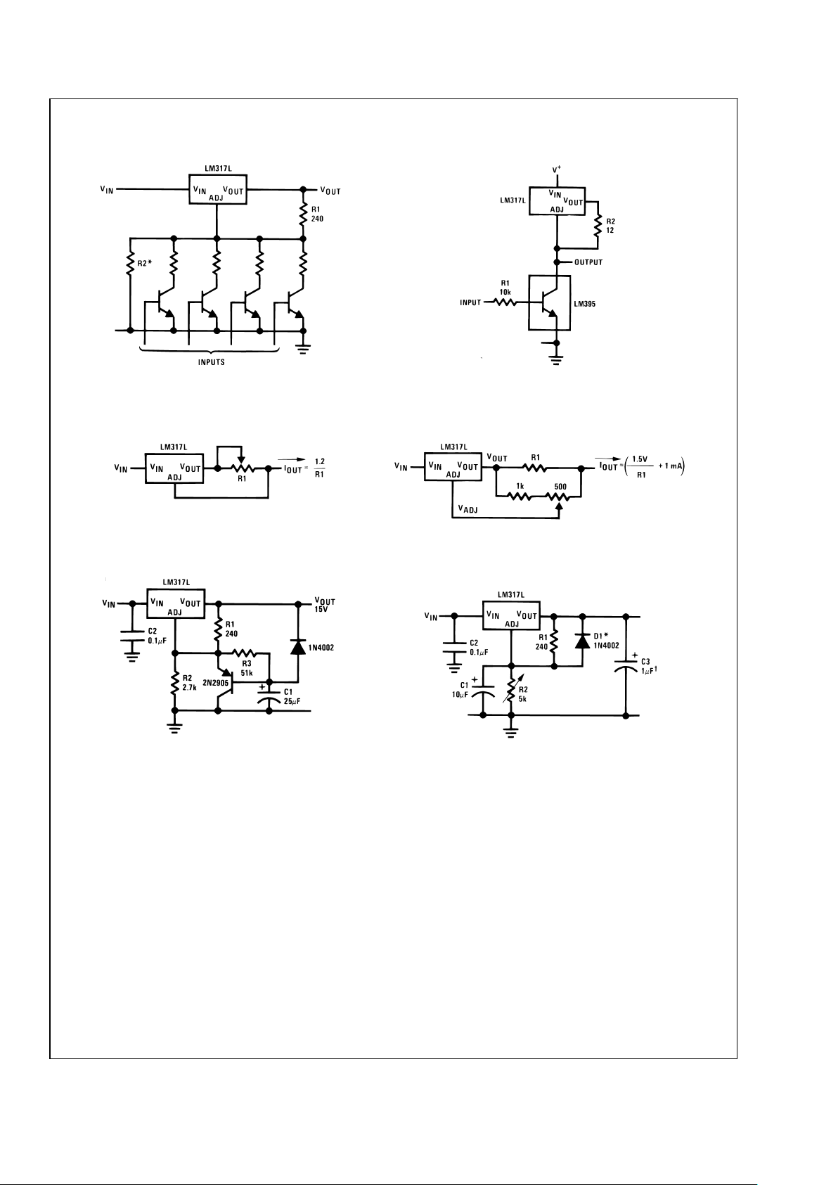
Typical Applications
Digitally Selected Outputs
DS009064-11
*Sets maximum V
OUT
High Gain Amplifier
DS009064-12
Adjustable Current Limiter
DS009064-13
12 ≤ R1 ≤ 240
Precision Current Limiter
DS009064-14
Slow Turn-On 15V Regulator
DS009064-15
Adjustable Regulator with
Improved Ripple Rejection
DS009064-16
†
Solid tantalum
*
Discharges C1 if output is shorted to ground
LM317L
www.national.com9

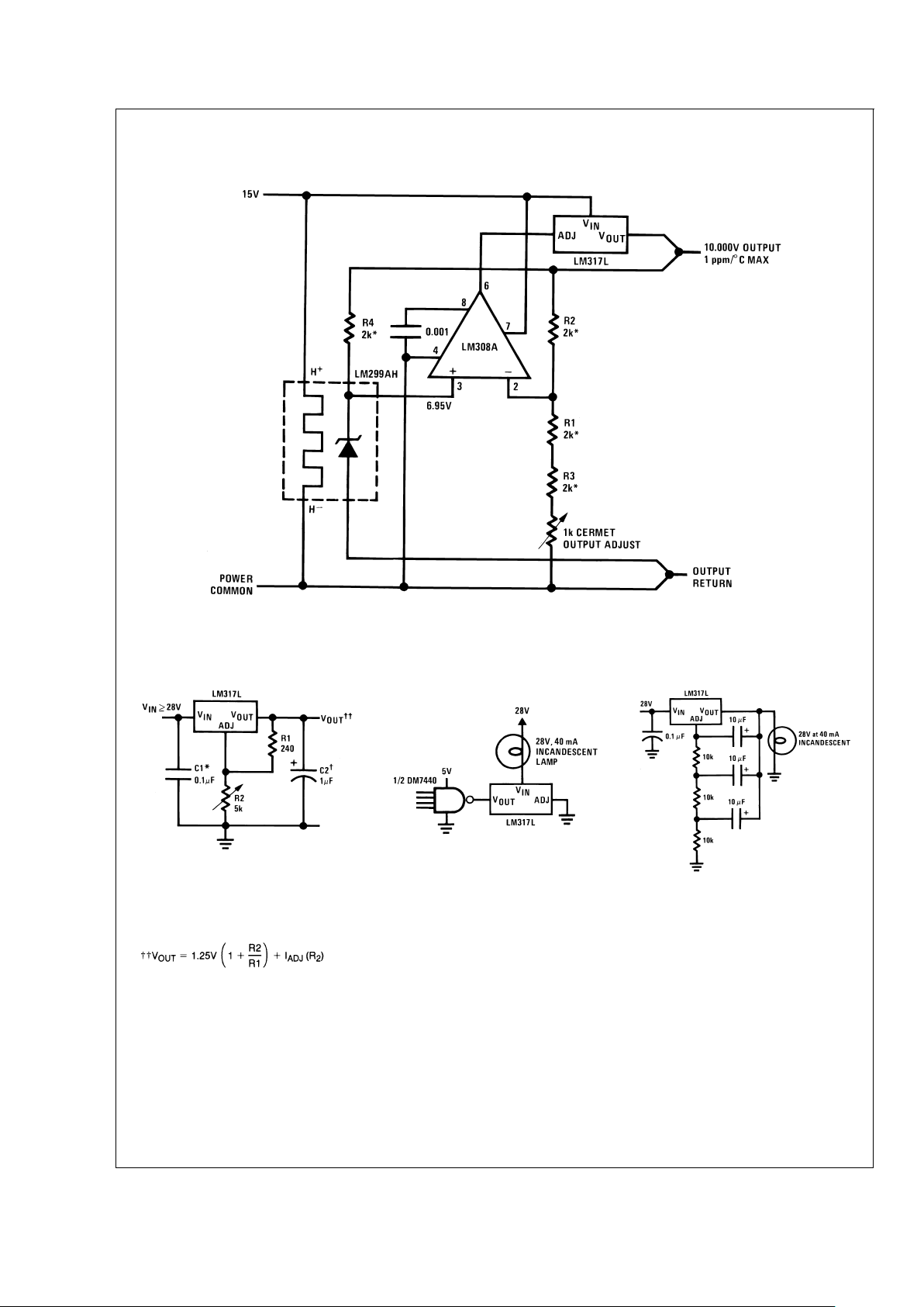
Typical Applications (Continued)
High Stability 10V Regulator
DS009064-17
Adjustable Regulator with Current Limiter
DS009064-18
Short circuit current is approximately 600 mV/R3, or 60mA (compared to
LM317LZ’s 200mA current limit).
At 25mA output only 3/4V of drop occurs in R3 and R4.
0V–30V Regulator
DS009064-19
Full output current not available at high
input-output voltages
Regulator With 15mA Short Circuit
Current
DS009064-20
Power Follower
DS009064-21
Adjusting Multiple On-Card Regulators with Single Control
*
DS009064-22
*
All outputs within±100mV
†
Minimum load −5mA
LM317L
www.national.com 10

Typical Applications (Continued)
100mA Current Regulator
DS009064-23
1.2V–12V Regulator with Minimum
Program Current
DS009064-24
*
Minimum load current ≈ 2mA
50mA Constant Current Battery
Charger for Nickel-Cadmium
Batteries
DS009064-25
5V Logic Regulator with Electronic Shutdown
*
DS009064-26
*
Minimum output ≈ 1.2V
Current Limited 6V Charger
DS009064-27
*
Sets peak current, I
PEAK
= 0.6V/R1
**
1000µF is recommended to filter out any input transients.
LM317L
www.national.com11

Typical Applications (Continued)
Short Circuit Protected 80V Supply
DS009064-28
Basic High Voltage Regulator
DS009064-29
Q1, Q2: NSD134 or similar
C1, C2: 1µF, 200V mylar
**
*
Heat sink
LM317L
www.national.com 12

Typical Applications (Continued)
Precision High Voltage Regulator
DS009064-30
Q1, Q2: NSD134 or similar
C1, C2: 1µF, 200V mylar
**
*
Heat sink
**
Mylar is a registered trademark of DuPont Co.
Tracking Regulator
DS009064-31
A1 = LM301A, LM307, or LF13741 only
R1, R2 = matched resistors with good TC tracking
Regulator With Trimmable Output Voltage
DS009064-32
Trim Procedure:
—If V
OUT
is 23.08V or higher, cut out R3 (if lower, don’t cut it out).
—Then if V
OUT
is 22.47V or higher, cut out R4 (if lower, don’t).
—Then if V
OUT
is 22.16V or higher, cut out R5 (if lower, don’t).
This will trim the output to well within
±
1% of 22.00 VDC, without any of
the expense or uncertainty of a trim pot (see LB-46). Of course, this
technique can be used at any output voltage level.
LM317L
www.national.com13
Typical Applications (Continued)
Precision Reference with Short-Circuit Proof Output
DS009064-33
*
R1–R4 from thin-film network,
Beckman 694-3-R2K-D or similar
1.2V-25 Adjustable Regulator
DS009064-1
Full output current not available at high
input-output voltages
†
Optional—improves transient response
*Needed if device is more than 6 inches from
filter capacitors
Fully Protected (Bulletproof)
Lamp Driver
DS009064-2
Lamp Flasher
DS009064-3
Output rate — 4 flashes per second at 10% duty
cycle
LM317L
www.national.com 14

Physical Dimensions inches (millimeters) unless otherwise noted
SO-8 Molded Package
NS Package Number M08A
TO-92 Plastic Package (Z)
NS Package Number Z03A
LM317L
www.national.com15

Physical Dimensions inches (millimeters) unless otherwise noted (Continued)
NOTE: UNLESS OTHERWISE SPECIFIED.
1. EPOXY COATING
2. 63Sn/37Pb EUTECTIC BUMP.
3. RECOMMEND NON-SOLDER MASK DEFINED LANDING PAD.
4. PIN 1 IS ESTABLISHED BY LOWER LEFT CORNER WITH RESPECT TO TEXT ORIENTATION PINS ARE NUMBERED
COUNTERCLOCKWISE.
5. XXX IN DRAWING NUMBER REPRESENTS PACKAGE SIZE VARIATION WHERE X
1
IS PACKAGE WIDTH, X2IS PACK-
AGE LENGTH AND X
3
IS PACKAGE HEIGHT.
6. REFERENCE JEDEC REGISTRATION MO-211, VARIATION BC.
6-Bump micro SMD
NS Package Number BPA06HPA
X
1
= 0.955 X2= 1.615 X3=0.700
LM317L
www.national.com 16

Notes
LIFE SUPPORT POLICY
NATIONAL’S PRODUCTS ARE NOT AUTHORIZED FOR USE AS CRITICAL COMPONENTS IN LIFE SUPPORT
DEVICES OR SYSTEMS WITHOUT THE EXPRESS WRITTEN APPROVAL OF THE PRESIDENT AND GENERAL
COUNSEL OF NATIONAL SEMICONDUCTOR CORPORATION. As used herein:
1. Life support devices or systems are devices or
systems which, (a) are intended for surgical implant
into the body, or (b) support or sustain life, and
whose failure to perform when properly used in
accordance with instructions for use provided in the
labeling, can be reasonably expected to result in a
significant injury to the user.
2. A critical component is any component of a life
support device or system whose failure to perform
can be reasonably expected to cause the failure of
the life support device or system, or to affect its
safety or effectiveness.
National Semiconductor
Corporation
Americas
Tel: 1-800-272-9959
Fax: 1-800-737-7018
Email: support@nsc.com
National Semiconductor
Europe
Fax: +49 (0) 180-530 85 86
Email: europe.support@nsc.com
Deutsch Tel: +49 (0) 69 9508 6208
English Tel: +44 (0) 870 24 0 2171
Français Tel: +33 (0) 1 41 91 8790
National Semiconductor
Asia Pacific Customer
Response Group
Tel: 65-2544466
Fax: 65-2504466
Email: ap.support@nsc.com
National Semiconductor
Japan Ltd.
Tel: 81-3-5639-7560
Fax: 81-3-5639-7507
www.national.com
LM317L 3-Terminal Adjustable Regulator
National does not assume any responsibility for use of any circuitry described, no circuit patent licenses are implied and National reserves the right at any time without notice to change said circuitry and specifications.
 Loading...