NSC LM310N, LM310J, LM310H, LM210J, LM110N Datasheet
...
TL/H/7761
LM110/LM210/LM310 Voltage Follower
November 1994
LM110/LM210/LM310 Voltage Follower
General Description
The LM110 series are monolithic operational amplifiers internally connected as unity-gain non-inverting amplifiers.
They use super-gain transistors in the input stage to get low
bias current without sacrificing speed. Directly interchangeable with 101, 741 and 709 in voltage follower applications,
these devices have internal frequency compensation and
provision for offset balancing.
The LM110 series are useful in fast sample and hold circuits, active filters, or as general-purpose buffers. Further,
the frequency response is sufficiently better than standard
IC amplifiers that the followers can be included in the feedback loop without introducing instability. They are plug-in
replacements for the LM102 series voltage followers, offer-
ing lower offset voltage, drift, bias current and noise in addition to higher speed and wider operating voltage range.
The LM110 is specified over a temperature range
b
55§C
s
T
A
s
a
125§C, the LM210 fromb25§CsT
A
s
a
85§C and
the LM310 from 0
§
CsT
A
s
a
70§C.
Features
Y
Input current 10 nA max over temperature
Y
Small signal bandwidth 20 MHz
Y
Slew rate 30 V/ms
Y
Supply voltage range
g
5V tog18V
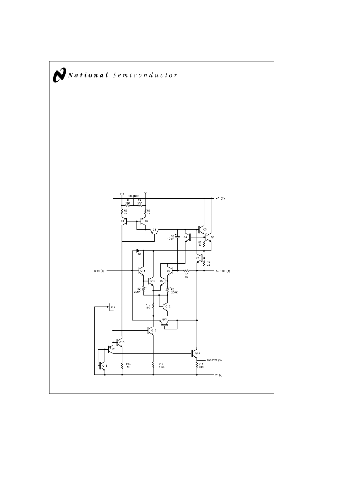
Schematic Diagram
TL/H/7761– 1
C
1995 National Semiconductor Corporation RRD-B30M115/Printed in U. S. A.

Absolute Maximum Ratings
If Military/Aerospace specified devices are required,
please contact the National Semiconductor Sales
Office/Distributors for availability and specifications.
(Note 6)
Supply Voltage
g
18V
Power Dissipation (Note 1) 500 mW
Input Voltage (Note 2)
g
15V
Output Short Circuit Duration (Note 3) Indefinite
Operating Temperature Range
LM110
b
55§Ctoa125§C
LM210
b
25§Ctoa85§C
LM310 0
§
Ctoa70§C
Storage Temperature Range
b
65§Ctoa150§C
Lead Temperature (Soldering, 10 sec.) 260§C
Soldering Information
Dual-In-Line Package
Soldering (10 sec.) 260
§
C
Small Outline Package
Vapor Phase (60 sec.) 215
§
C
Infrared (15 sec.) 220
§
C
See AN-450 ‘‘Surface Mounting Methods and Their Effect
on Product Reliability’’ for other methods of soldering surface mount devices.
ESD rating to be determined.
Electrical Characteristics (Note 4)
Parameter Conditions
LM110 LM210 LM310
Units
Min Typ Max Min Typ Max Min Typ Max
Input Offset Voltage T
A
e
25§C 1.5 4.0 1.5 4.0 2.5 7.5 mV
Input Bias Current T
A
e
25§C 1.0 3.0 1.0 3.0 2.0 7.0 nA
Input Resistance T
A
e
25§C10
101012
101010
12
101010
12
X
Input Capacitance 1.5 1.5 1.5 pF
Large Signal Voltage T
A
e
25§C, V
S
e
g
15V
0.999 0.9999 0.999 0.9999 0.999 0.9999 V/V
Gain V
OUT
e
g
10V, R
L
e
8kX
Output Resistance T
A
e
25§C 0.75 2.5 0.75 2.5 0.75 2.5 X
Supply Current T
A
e
25§C 3.9 5.5 3.9 5.5 3.9 5.5 mA
Input Offset Voltage 6.0 6.0 10 mV
Offset Voltage
b
55§CsT
A
s
a
85§C6 6 mV/§C
Temperature Drift
a
85sT
A
s
125§C12 mV/§C
0
§
CsT
A
s
a
70§C10mV/§C
Input Bias Current 10 10 10 nA
Large Signal Voltage V
S
e
g
15V, V
OUT
e
g
10V
0.999 0.999 0.999 V/V
Gain R
L
e
10 kX
Output Voltage V
S
e
g
15V, R
L
e
10 kX
g
10
g
10
g
10 V
Swing (Note 5)
Supply Current T
A
e
125§C 2.0 4.0 2.0 4.0 mA
Supply Voltage
g
5VsV
S
s
g
18V
70 80 70 80 70 80 dB
Rejection Ratio
Note 1: The maximum junction temperature of the LM110 is 150§C, of the LM210 is 100§C, and of the LM310 is 85§C. For operating at elevated temperatures,
devices in the HO8 package must be derated based on a thermal resistance of 165
§
C/W, junction to ambient, or 22§C/W, junction to case. The thermal resistance
of the dual-in-line package is 100
§
C/W, junction to ambient.
Note 2: For supply voltages less than
g
15V, the absolute maximum input voltage is equal to the supply voltage.
Note 3: Continuous short circuit for the LM110 and LM210 is allowed for case temperatures to 125
§
C and ambient temperatures to 70§C, and for the LM310, 70§C
case temperature or 55
§
C ambient temperature. It is necessary to insert a resistor greater than 2 kX in series with the input when the amplifier is driven from low
impedance sources to prevent damage when the output is shorted. R
S
e
5k min, 10k typical is recommended for dynamic stability in all applications.
Note 4: These specifications apply for
g
5VsV
S
s
g
18V andb55§CsTA125§C for the LM110,b25§CsT
A
s
85§C for the LM210, and 0§CsT
A
s
70§C for
the LM310 unless otherwise specified.
Note 5: Increased output swing under load can be obtained by connecting an external resistor between the booster and V
b
terminals. See curve.
Note 6: Refer to RETS110X for LM110H, LM110J military specifications.
Application Hint
The input must be driven from a source impedance of typically 10 kX (5 kX min.) to maintain stability. The total source
impedance will be reduced at high frequencies if there is stray capacitance at the input pin. In these cases, a 10 kX resistor
should be inserted in series with the input, physically close to the input pin to minimize the stray capacitance and prevent
oscillation.
2

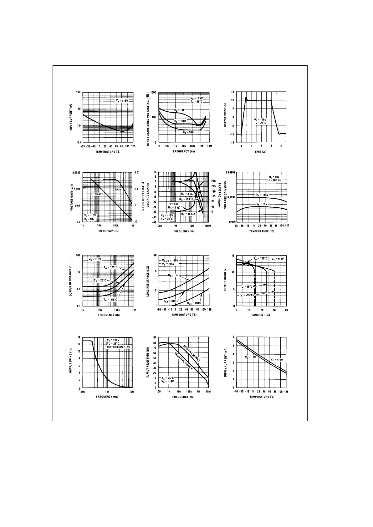
Typical Performance Characteristics (LM110/LM210)
Input Current Output Noise Voltage Response
Large Signal Pulse
Phase Lag
Voltage Gain and
Phase Lag
Voltage Gain and
Voltage Gain
Output Resistance Symmetrical Output Swing Positive Output Swing
Frequency Response
Large Signal
Power Supply Rejection Supply Current
TL/H/7761– 28
3

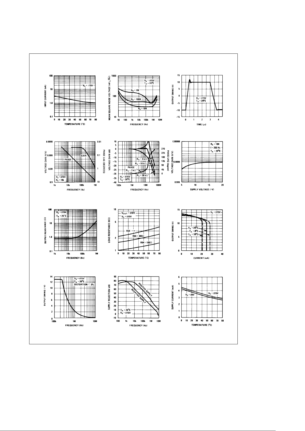
Typical Performance Characteristics (LM310)
Input Current Output Noise Voltage Response
Large Signal Pulse
Phase Lag
Voltage Gain and
Phase Lag
Voltage Gain and
Voltage Gain
Output Resistance Symmetrical Output Swing Positive Output Swing
Frequency Response
Large Signal
Power Supply Rejection Supply Current
TL/H/7761– 29
4

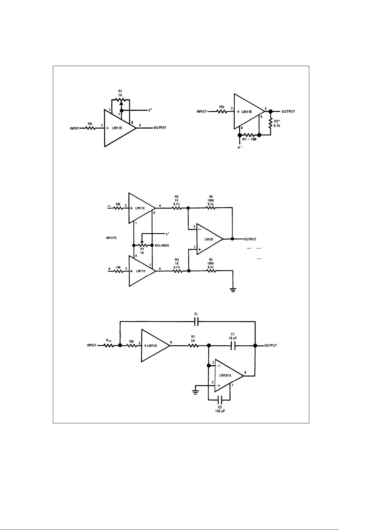
Auxiliary Circuits
Offset Balancing Circuit
TL/H/7761– 2
Increasing Negative Swing Under Load
TL/H/7761– 3
*May be added to reduce internal dissipation
Typical Applications
Differential Input Instrumentation Amplifier
TL/H/7761– 4
R4
R2
e
R5
R3
A
V
e
R4
R2
Fast Integrator with Low Input Current
TL/H/7761– 5
5
 Loading...