

NSC LM3102MHX, LM3102 Datasheet
September 2007
LM3102
SIMPLE SWITCHER® Synchronous 1MHz 2.5A
Step-Down Voltage Regulator
General Description
The LM3102 Synchronously Rectified Buck Converter features all required functions to implement a highly efficient and
cost effective buck regulator. It is capable of supplying 2.5A
to loads with an output voltage as low as 0.8V. Dual N-Channel synchronous MOSFET switches allow a low component
count, thus reducing complexity and minimizing board size.
Different from most other COT regulators, the LM3102 does
not rely on output capacitor ESR for stability, and is designed
to work exceptionally well with ceramic and other very low
ESR output capacitors. It requires no loop compensation, results in a fast load transient response and simple circuit
implementation. The operating frequency remains nearly constant with line variations due to the inverse relationship between the input voltage and the on-time. The operating
frequency can be externally programmed up to 1 MHz. Protection features include VCC under-voltage lock-out, output
over-voltage protection, thermal shutdown, and gate drive
under-voltage lock-out. The LM3102 is available in the thermally enhanced eTSSOP-20 package.
Key Specifications
■
Input voltage range 4.5V-42V
■
2.5A output current
■
0.8V, ±1.5% reference
■
Integrated dual N-Channel main and synchronous
MOSFETs
■
Thermally enhanced eTSSOP-20 package
Features
■
Low component count and small solution size
■
Stable with ceramic and other low ESR capacitors
■
No loop compensation required
■
High efficiency at a light load by DCM operation
■
Pre-bias startup
■
Ultra-fast transient response
■
Programmable soft-start
■
Programmable switching frequency up to 1 MHz
■
Valley current limit
■
Output over-voltage protection
■
Precision internal reference for an adjustable output
voltage down to 0.8V
■
Thermal shutdown
Typical Applications
■
5VDC, 12VDC, 24VDC, 12VAC, and 24VAC systems
■
Embedded Systems
■
Industrial Control
■
Automotive Telematics and Body Electronics
■
Point of Load Regulators
■
Storage Systems
■
Broadband Infrastructure
■
Direct Conversion from 2/3/4 Cell Lithium Batteries
Systems
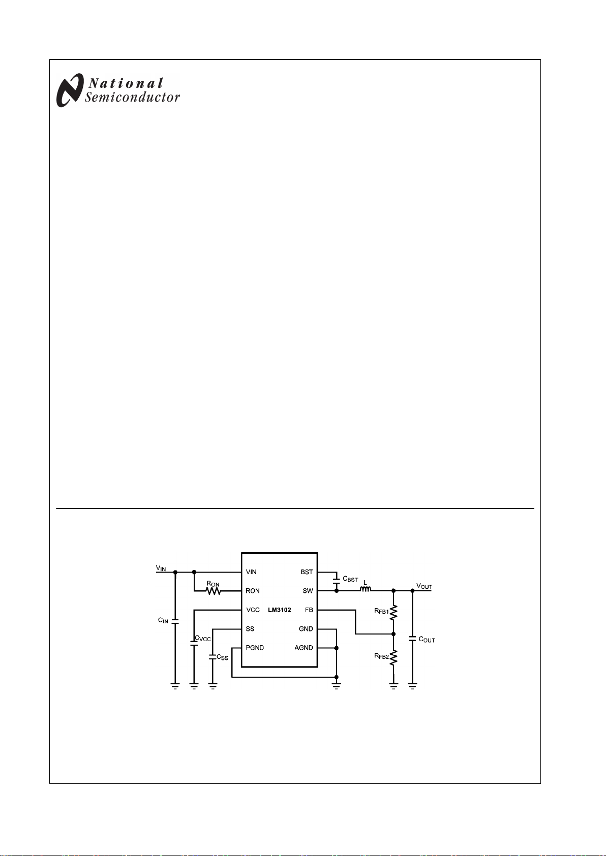
Typical Application
30021301
SIMPLE SWITCHER® is a registered trademark of National Semiconductor Corporation
© 2007 National Semiconductor Corporation 300213 www.national.com
LM3102 SIMPLE SWITCHER® Synchronous 1MHz 2.5A Step-Down Voltage Regulator
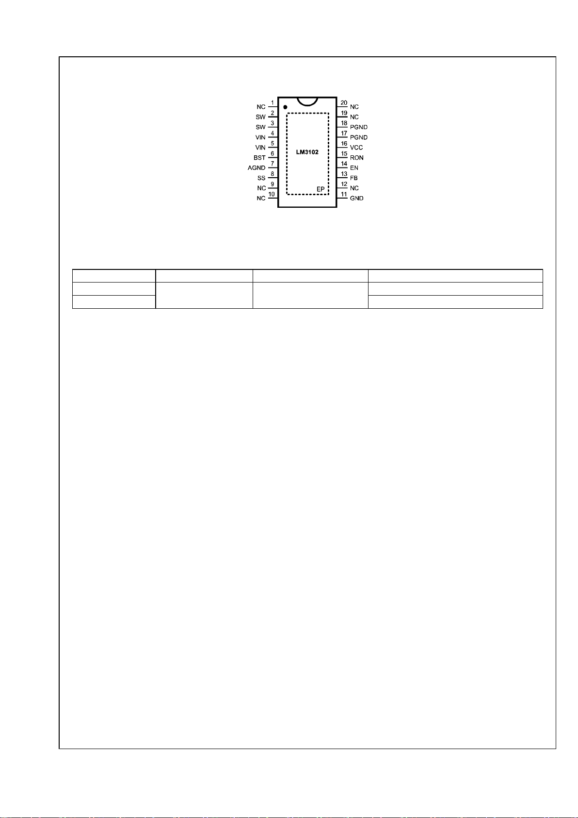
Connection Diagram
30021302
20-lead Plastic eTSSOP
NS Package Number MXA20A
Ordering Information
Order Number Package Type NSC Package Drawing Supplied As
LM3102MH Exposed Pad TSSOP-20 MXA0020 73 units per Anti-Static Tube
LM3102MHX 2500 Units on Tape and Reel
www.national.com 2
LM3102
Pin Descriptions
Pin Name Description Application Information
1,9,10,12,19,20 N/C No Connection These pins must be left unconnected.
2, 3 SW Switching Node Internally connected to the source of the main
MOSFET and the drain of the Synchronous MOSFET.
Connect to the inductor.
4, 5 VIN Input supply voltage Supply pin to the device. Nominal input range is 4.5V
to 42V.
6 BST Connection for bootstrap capacitor Connect a 33 nF capacitor from the SW pin to this pin.
An internal diode charges the capacitor during the main
MOSFET off-time.
7 AGND Analog Ground Ground for all internal circuitry other than the PGND
pin.
8 SS Soft-start An 8 µA internal current source charges an external
capacitor to provide the soft- start function.
11 GND Ground Must be connected to the AGND pin for normal
operation. The GND and AGND pins are not internally
connected.
13 FB Feedback Internally connected to the regulation and over-voltage
comparators. The regulation setting is 0.8V at this pin.
Connect to feedback resistors.
14 EN Enable pin Connect a voltage higher than 1.26V to enable the
regulator.
15 RON On-time Control An external resistor from the VIN pin to this pin sets the
main MOSFET on-time.
16 VCC Start-up regulator Output Nominally regulated to 6V. Connect a capacitor of not
less than 680 nF between the VCC and AGND pins for
stable operation.
17, 18 PGND Power Ground Synchronous MOSFET source connection. Tie to a
ground plane.
DAP EP Exposed Pad Thermal connection pad. Connect to the ground plane.
3 www.national.com
LM3102
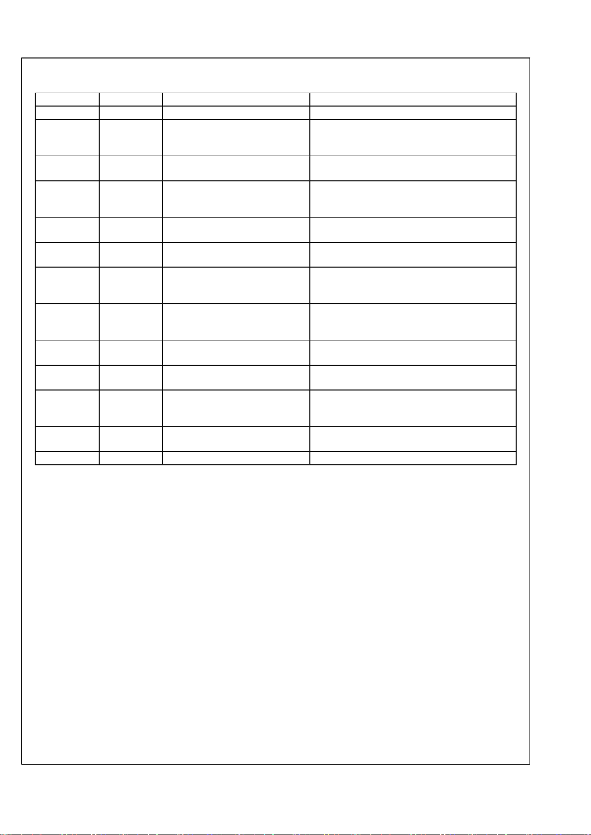
Absolute Maximum Ratings (Note 1)
If Military/Aerospace specified devices are required,
please contact the National Semiconductor Sales Office/
Distributors for availability and specifications.
VIN, RON to AGND -0.3V to 43.5V
SW to AGND -0.3V to 43.5V
SW to AGND (Transient) -2V (< 100ns)
VIN to SW -0.3V to 43.5V
BST to SW -0.3V to 7V
All Other Inputs to AGND -0.3V to 7V
ESD Rating (Note 2)
Human Body Model ±2kV
Storage Temperature Range -65°C to +150°C
Junction Temperature (TJ) 150°C
Operating Ratings (Note 1)
Supply Voltage Range (VIN) 4.5V to 42V
Junction Temperature Range (TJ)
−40°C to +125°C
Thermal Resistance (θJC) (Note 3)
6.5°C/W
Electrical Characteristics Specifications with standard type are for T
J
= 25°C only; limits in boldface type apply
over the full Operating Junction Temperature (TJ) range. Minimum and Maximum limits are guaranteed through test, design, or
statistical correlation. Typical values represent the most likely parametric norm at TJ = 25°C, and are provided for reference
purposes only. Unless otherwise stated the following conditions apply: VIN = 18V, V
OUT
= 3.3V.
Symbol Parameter Conditions Min Typ Max Units
Start-Up Regulator, V
CC
V
CC
VCC output voltage CCC = 680nF, no load 5.0 6.0 7.2 V
VIN - V
CC
V
IN
- VCC dropout voltage ICC = 2mA 50 200 mV
ICC = 20mA 350 570
I
VCCL
VCC current limit (Note 4) VCC = 0V 40 65 mA
V
CC-UVLO
VCC under-voltage lockout threshold
(UVLO)
VIN increasing 3.6 3.75 3.9 V
V
CC-UVLO-HYS
VCC UVLO hysteresis VIN decreasing 130 mV
t
VCC-UVLO-D
VCC UVLO filter delay 3 µs
I
IN
IIN operating current No switching, VFB = 1V 0.7 1 mA
I
IN-SD
IIN operating current, Device shutdown VEN = 0V 25 40 µA
Switching Characteristics
R
DS-UP-ON
Main MOSFET R
DS(on)
0.18 0.375
Ω
R
DS- DN-ON
Syn. MOSFET R
DS(on)
0.11 0.225
Ω
V
G-UVLO
Gate drive voltage UVLO V
BST
- VSW increasing 3.3 4 V
Soft-start
I
SS
SS pin source current VSS = 0.5V 6 8 10 µA
Current Limit
I
CL
Syn. MOSFET current limit threshold 2.7 A
ON/OFF Timer
t
on
ON timer pulse width
VIN = 10V, RON = 100 kΩ
1.38 µs
VIN = 30V, RON = 100 kΩ
0.47
t
on-MIN
ON timer minimum pulse width 150 ns
t
off
OFF timer pulse width 260 ns
Enable Input
V
EN
EN Pin input threshold VEN rising 1.13 1.18 1.23 V
V
EN-HYS
Enable threshold hysteresis VEN falling 90 mV
Regulation and Over-Voltage Comparator
V
FB
In-regulation feedback voltage
VSS ≥ 0.8V
TJ = −40°C to +125°C
0.784 0.8 0.816 V
VSS ≥ 0.8V
TJ = 0°C to +125°C
0.788 0.812
V
FB-OV
Feedback over-voltage threshold 0.888 0.920 0.945 V
I
FB
5 nA
www.national.com 4
LM3102
Symbol Parameter Conditions Min Typ Max Units
Thermal Shutdown
T
SD
Thermal shutdown temperature TJ rising 165 °C
T
SD-HYS
Thermal shutdown temperature
hysteresis
TJ falling 20 °C
Note 1: Absolute Maximum Ratings are limits beyond which damage to the device may occur. Operating Ratings are conditions under which operation of the
device is intended to be functional. For guaranteed specifications and test conditions, see the Electrical Characteristics.
Note 2: The human body model is a 100pF capacitor discharged through a 1.5kΩ resistor into each pin.
Note 3: θJC measurements are performed in general accordance with Mil-Std 883B, Method 1012.1 and utilizes the copper heat sink technique. Copper Heat
Sink @ 60°C.
Note 4: VCC provides self bias for the internal gate drive and control circuits. Device thermal limitations limit external loading.
5 www.national.com
LM3102
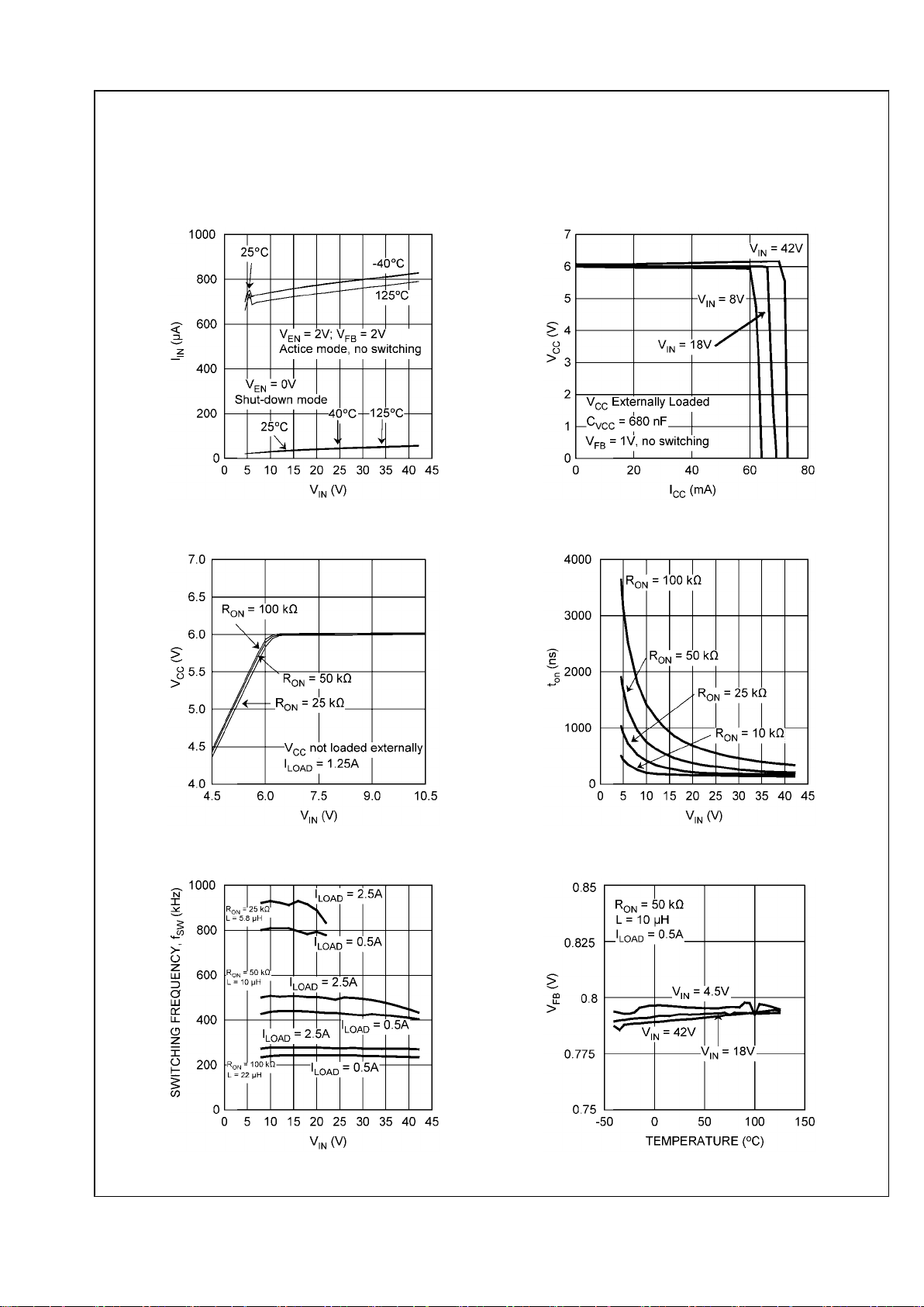
Typical Performance Characteristics
All curves are taken at VIN = 18V with the configuration in the typical application circuit for V
OUT
= 3.3V shown in this datasheet.
TA = 25°C, unless otherwise specified.
Quiescent Current, IIN vs V
IN
30021303
VCC vs I
CC
30021304
VCC vs V
IN
30021305
ton vs V
IN
30021306
Switching Frequency, fSW vs V
IN
30021307
VFB vs Temperature
30021308
www.national.com 6
LM3102
 Loading...