

LM3100
SIMPLE SWITCHER
®
Synchronous 1MHz 1.5A
Step-Down Voltage Regulator
LM3100 SIMPLE SWITCHER
February 2006
General Description
The LM3100 Synchronously Rectified Buck Converter features all functions needed to implement a highly efficient,
cost effective buck regulator capable of supplying 1.5A to
loads with voltages as low as 0.8V. Dual 40V N-Channel
synchronous MOSFET switches allow for low external component thus reducing complexity and minimizing board
space. The LM3100 is designed to work exceptionally well
with ceramic and other very low ESR output capacitors. The
Constant ON-Time (COT) regulation scheme requires no
loop compensation, results in fast load transient response,
and simplifies circuit implementation. Through the use of a
unique design the regulator does not rely on output capacitor
ESR for stability, as do most other COT regulators. The
operating frequency remains nearly constant with line and
load variations due to the inverse relationship between the
input voltage and the on-time. The oprating frequency can
be externally programmed up to 1MHz. Protection features
include V
gate drive under-voltage lockout. The part is available in a
thermally enhanced eTSSOP-20 package
under-voltage lockout, thermal shutdown and
CC
Features
n Input voltage range 4.5V - 36V
n 1.5A output current
n 0.8V,
n Integrated 40V, dual N-Channel buck synchronous
n Low component count and small solution size
n No loop compensation required
n Ultra-fast transient response
n Stable with ceramic and other low ESR capacitors
n Programmable switching frequency up to 1MHz
n Max. duty cycle limited during start-up
n Valley current limit
n Precision Internal Reference for adjustable output
n Thermal shutdown
n Thermally enhanced eTSSOP-20 package
±
1.5% reference
switches
voltage down to 0.8V
Typical Applications
n 5VDC, 12VDC, 24VDC, 12VAC, and 24VAC systems
n Embedded Systems
n Industrial Controls
n Automotive Telematics and Body Electronics
n Point of Load Regulators
n Storage Systems
n Broadband Infrastructure
n Direct Conversion from 2/3/4 Cell Lithium Batteries
Systems
®
Synchronous 1MHz 1.5A Step-Down Voltage Regulator
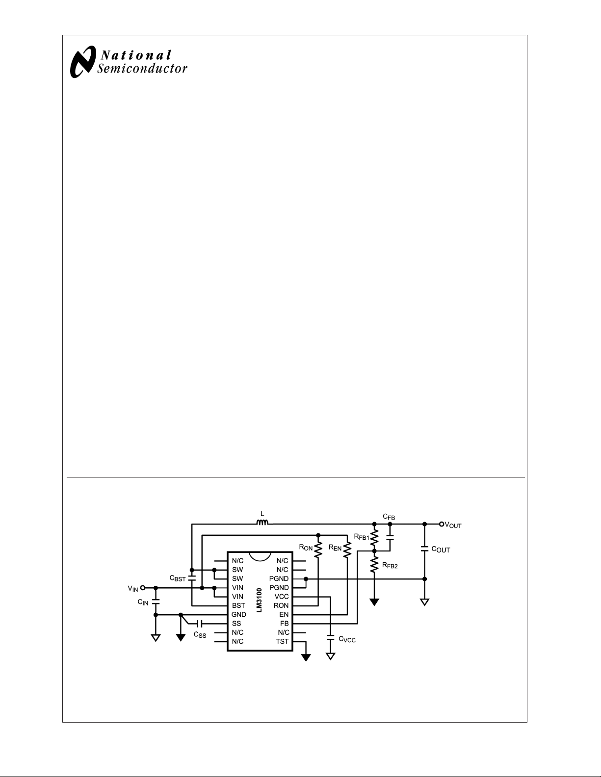
Typical Application
20174702
SIMPLE SWITCHER®is a registered trademark of National Semiconductor Corporation
© 2006 National Semiconductor Corporation DS201747 www.national.com
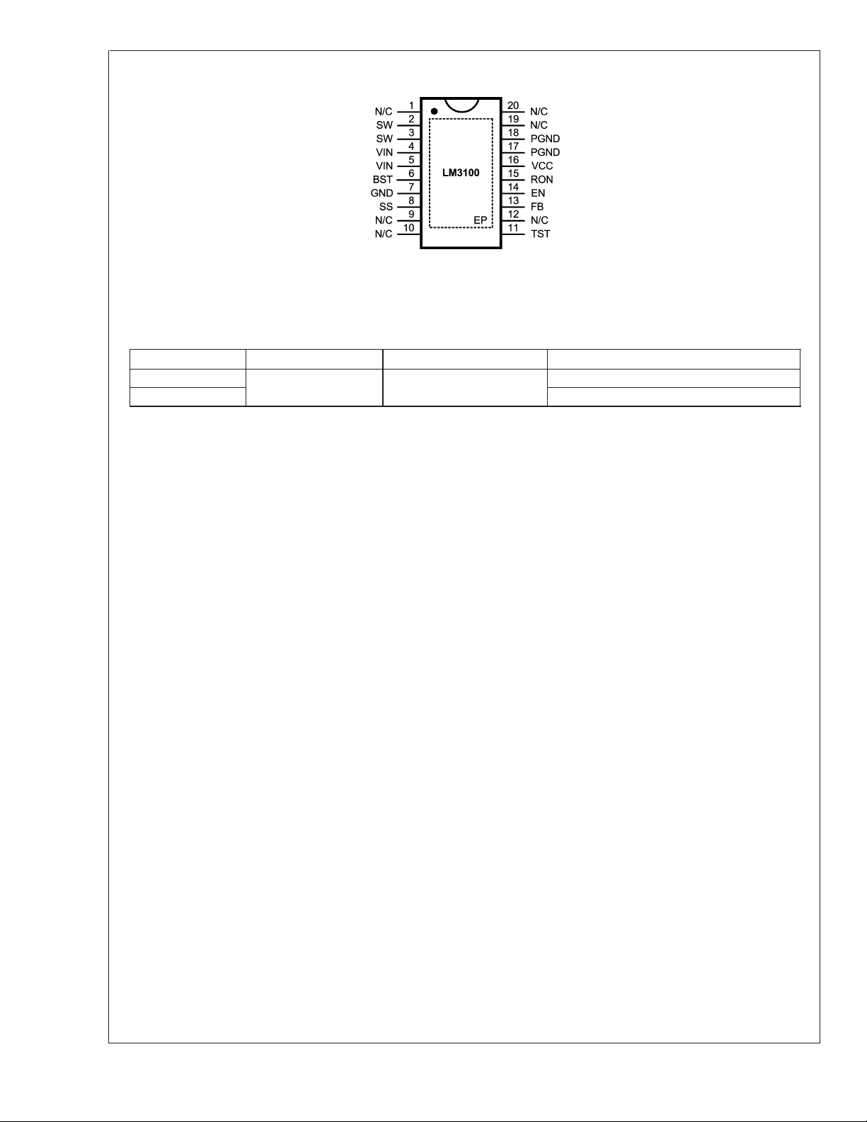
Connection Diagram
LM3100
20-lead Plastic
eTSSOP (MXA20A)
20174703
Ordering Information
Order Number Package Type NSC Package Drawing Supplied As
LM3100MH Exposed Pad
LM3100MHX 2500 Units on Tape and Reel
TSSOP-20
MXA0020 73 units per Anti-Static Tube
www.national.com 2
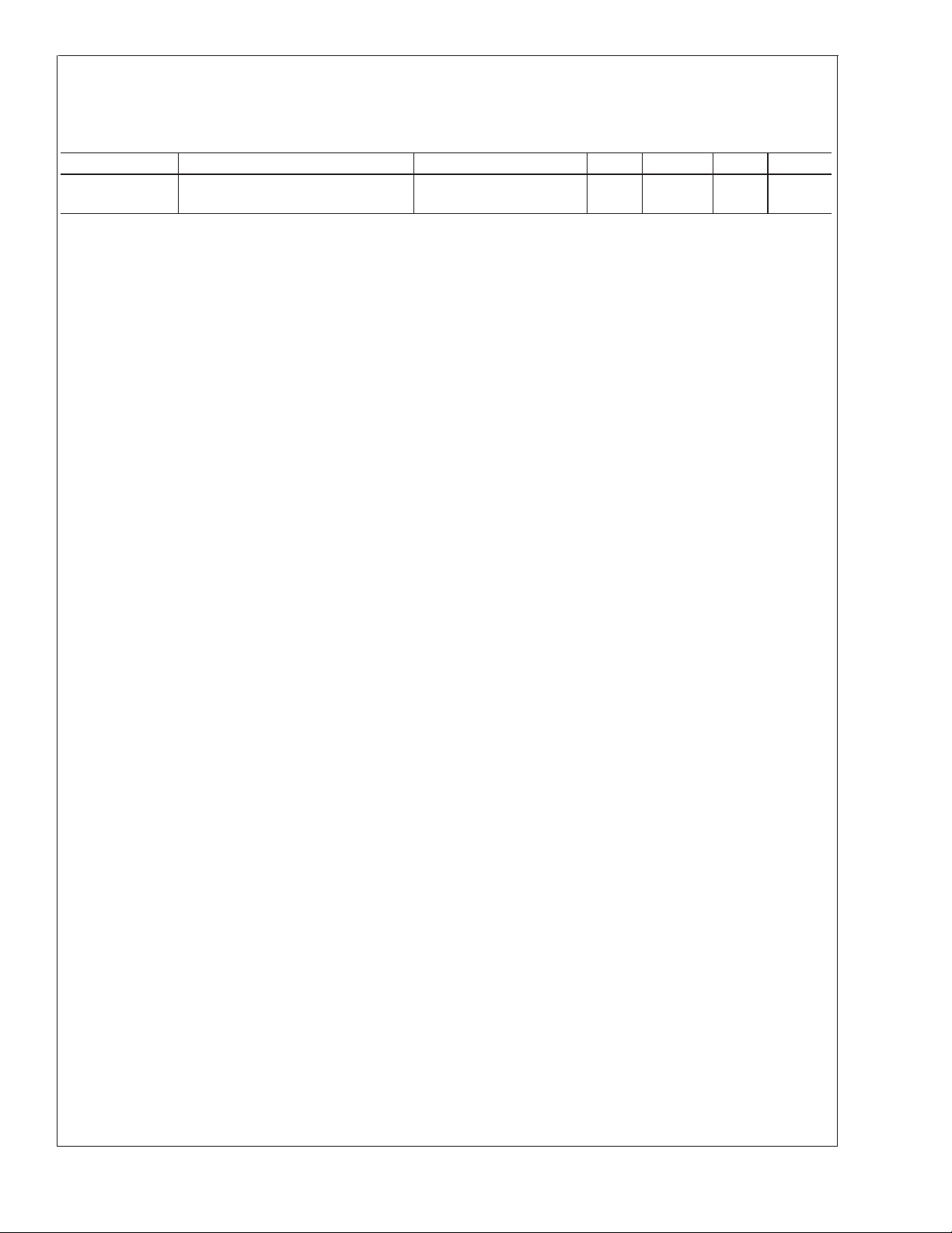
Pin Descriptions
Pin Name Description Application Information
1,9,10,12,19,20 N/C No Connection These pins must be left unconnected.
2, 3 SW Switching Node Internally connected to the buck switch source.
Connect to output inductor.
4, 5 VIN Input supply voltage Supply pin to the device. Nominal input range is
4.5V to 36V.
6 BST Connection for bootstrap capacitor Connect a 0.033µF capacitor from SW pin to this
pin. An internal diode charges the capacitor during
the high-side switch off-time.
7 GND Analog Ground Ground for all internal circuitry other than the
synchronous switches.
8 SS Soft-start An internal 8µA current source charges an external
capacitor to provide the soft- start function.
11 TST Test mode enable pin Force the device into test mode. Must be connected
to ground for normal operation.
13 FB Feedback Internally connected to the regulation and
over-voltage comparators. The regulation setting is
0.8V at this pin. Connect to feedback divider.
14 EN Enable pin Connect a voltage higher than 1.26V to enable the
regulator.
15 RON On-time Control An external resistor from VIN to this pin sets the
high-side switch on-time.
16 VCC Start-up regulator Output Nominally regulated to 6V. Connect a capacitor of
not less than 680nF between VCC and GND for
stable operation.
17, 18 PGND Power Ground Synchronous rectifier MOSFET source connection.
Tie to power ground plane.
DAP EP Exposed Pad Thermal connection pad, connect to GND.
LM3100
www.national.com3
Absolute Maximum Ratings (Note 1)
If Military/Aerospace specified devices are required,
LM3100
please contact the National Semiconductor Sales Office/
Distributors for availability and specifications.
VIN, RON to GND -0.3V to 40V
SW to GND -0.3V to 40V
SW to GND (Transient) -2V (
VIN to SW -0.3V to 40V
BST to SW -0.3V to 7V
All Other Inputs to GND -0.3V to 7V
<
100ns)
ESD Rating (Note 2)
Human Body Model
±
2kV
Storage Temperature Range -65˚C to +150˚C
Junction Temperature (T
) 150˚C
J
Operating Ratings (Note 1)
Supply Voltage Range (VIN) 4.5V to 36V
Junction Temperature Range (T
Thermal Resistance (θ
) (Note 3) 6.5˚C/W
JC
) −40˚C to + 125˚C
J
Electrical Charateristics Specifications with standard type are for T
ply over the full Operating Junction Temperature (T
sign, or statistical correlation. Typical values represent the most likely parametric norm at T
erence purposes only. Unless otherwise stated the following conditions apply: V
) range. Minimum and Maximum limits are guaranteed through test, de-
J
= 25˚C only; limits in boldface type ap-
J
= 25˚C, and are provided for ref-
= 18V, V
IN
J
OUT
= 3.3V.
Symbol Parameter Conditions Min Typ Max Units
Start-Up Regulator, V
V
CC
V
IN-VCC
I
VCCL
V
CC-UVLO
CC
VCCoutput voltage CCC= 680nF, no load 5.0 6.0 7.2 V
VIN-VCCdropout voltage ICC= 2mA 50 140 mV
I
= 20mA 350 570
CC
VCCcurrent limit (Note 4) VCC=0V 40 65 mA
VCCunder-voltage lockout threshold
VINincreasing 3.6 3.75 3.85 V
(UVLO)
V
CC-UVLO-HYS
t
VCC-UVLO-D
I
IN
I
IN-SD
VCCUVLO hysteresis VINdecreasing 130 mV
VCCUVLO filter delay 3 µs
IINoperating current No switching, VFB= 1V 0.7 1 mA
IINoperating current, Device shutdown VEN=0V 17 30 µA
Switching Characteristics
R
DS-UP-ON
R
DS- DN-ON
V
G-UVLO
Main MOSFET Rds(on) 0.18 0.35 Ω
Syn. MOSFET Rds(on) 0.11 0.2 Ω
Gate drive voltage UVLO V
BST-VSW
increasing 3.3 4 V
Soft-start
I
SS
SS pin source current VSS= 0.5V 6 8 9.8 µA
Current Limit
I
CL
Syn. MOSFET current limit threshold 1.9 A
ON/OFF Timer
t
ON
t
ON-MIN
t
OFF
ON timer pulse width VIN= 10V, RON= 100 kΩ 1.38 µs
V
= 30V, RON= 100 kΩ 0.47
IN
ON timer minimum pulse width 200 ns
OFF timer pulse width 260 ns
Enable Input
V
EN-HYS
V
EN
EN Pin input threshold VENrising 1.236 1.26 1.285 V
Enable threshold hysteresis VENfalling 90 mV
Regulation and Over-Voltage Comparator
V
V
FB
FB-OV
I
FB
In-regulation feedback voltage VSS≥ 0.8V
= −40˚C to + 125˚C
T
J
V
≥ 0.8V
SS
= 0˚C to + 125˚C
T
J
Feedback over-voltage threshold 0.894 0.920 0.940 V
0.784 0.8 0.816 V
0.788 0.812
5 100 nA
Thermal Shutdown
T
SD
Thermal shutdown temperature TJrising 165 ˚C
www.national.com 4
LM3100
Electrical Charateristics Specifications with standard type are for T
over the full Operating Junction Temperature (T
statistical correlation. Typical values represent the most likely parametric norm at T
purposes only. Unless otherwise stated the following conditions apply: V
) range. Minimum and Maximum limits are guaranteed through test, design, or
J
= 18V, V
IN
= 25˚C only; limits in boldface type apply
J
= 25˚C, and are provided for reference
J
= 3.3V. (Continued)
OUT
Symbol Parameter Conditions Min Typ Max Units
T
SD-HYS
Thermal shutdown temperature
TJfalling 20 ˚C
hysteresis
Note 1: Absolute Maximum Ratings are limits beyond which damage to the device may occur. Operating Ratings are conditions under which operation of the device
is intended to be functional. For guaranteed specifications and test conditions, see the Electrical Characteristics.
Note 2: The human body model is a 100pF capacitor discharged through a 1.5kΩ resistor into each pin.
Note 3: θ
@
60˚C.
Note 4: V
measurements are performed in general accordance with Mil-Std 883B, Method 1012.1 and utilizes the copper heat sink technique. Copper Heat Sink
JC
provides self bias for the internal gate drive and control circuits. Device thermal limitations limit external loading.
CC
www.national.com5

Typical Performance Characteristics All curves taken at V
plication circuit for V
LM3100
Quiescent Current, I
= 3.3V shown in this datasheet. TA= 25˚C, unless otherwise specified.
OUT
vs V
IN
IN
20174718 20174719
VCCvs V
IN
= 18V with configuration in typical ap-
IN
VCCvs I
TONvs V
CC
IN
20174720 20174721
Switching Frequency, FSWvs V
IN
20174722
www.national.com 6
VFBvs Temperature
20174723

LM3100
Typical Performance Characteristics All curves taken at V
application circuit for V
R
V
Regulation vs Load Current
OUT
= 3.3V shown in this datasheet. TA= 25˚C, unless otherwise specified. (Continued)
OUT
vs Temperature
DS(ON)
20174724
= 3.3V)
(V
OUT
= 18V with configuration in typical
IN
Efficiency vs Load Current
(V
= 3.3V)
OUT
Efficiency vs Load Current
(V
= 0.8V)
OUT
20174725
V
Regulation vs Load Current
OUT
(V
OUT
= 0.8V)
20174726 20174727
Power Up
(V
= 3.3V, 1.5A Loaded)
OUT
20174729
20174728
www.national.com7
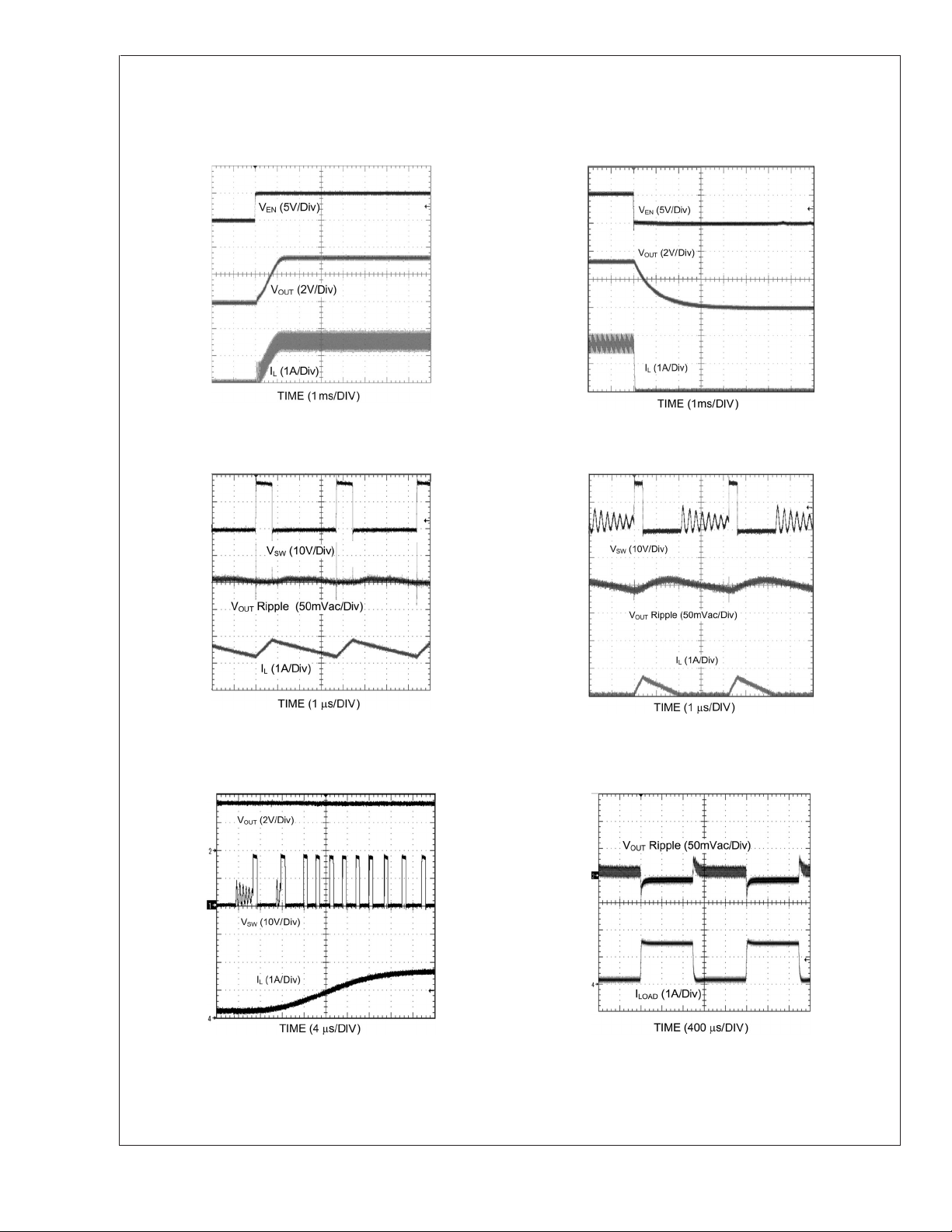
Typical Performance Characteristics All curves taken at V
application circuit for V
LM3100
(V
OUT
= 3.3V shown in this datasheet. TA= 25˚C, unless otherwise specified. (Continued)
OUT
Enable Transient
= 3.3V, 1.5A Loaded)
= 18V with configuration in typical
IN
Shutdown Transient
(V
= 3.3V, 1.5A Loaded)
OUT
Continuous Mode Operation
= 3.3V, 1.5A Loaded)
(V
OUT
CCM to DCM Transition
= 3.3V, 0.15A - 1.5A Load)
(V
OUT
20174730
20174732
Discontinuous Mode Operation
(V
= 3.3V, 1.5A Loaded)
OUT
Load Transient
(V
= 3.3V, 0.15A - 1.5A Load, Current slew-rate:
OUT
2.5A/µs)
20174731
20174733
20174734
www.national.com 8
20174735
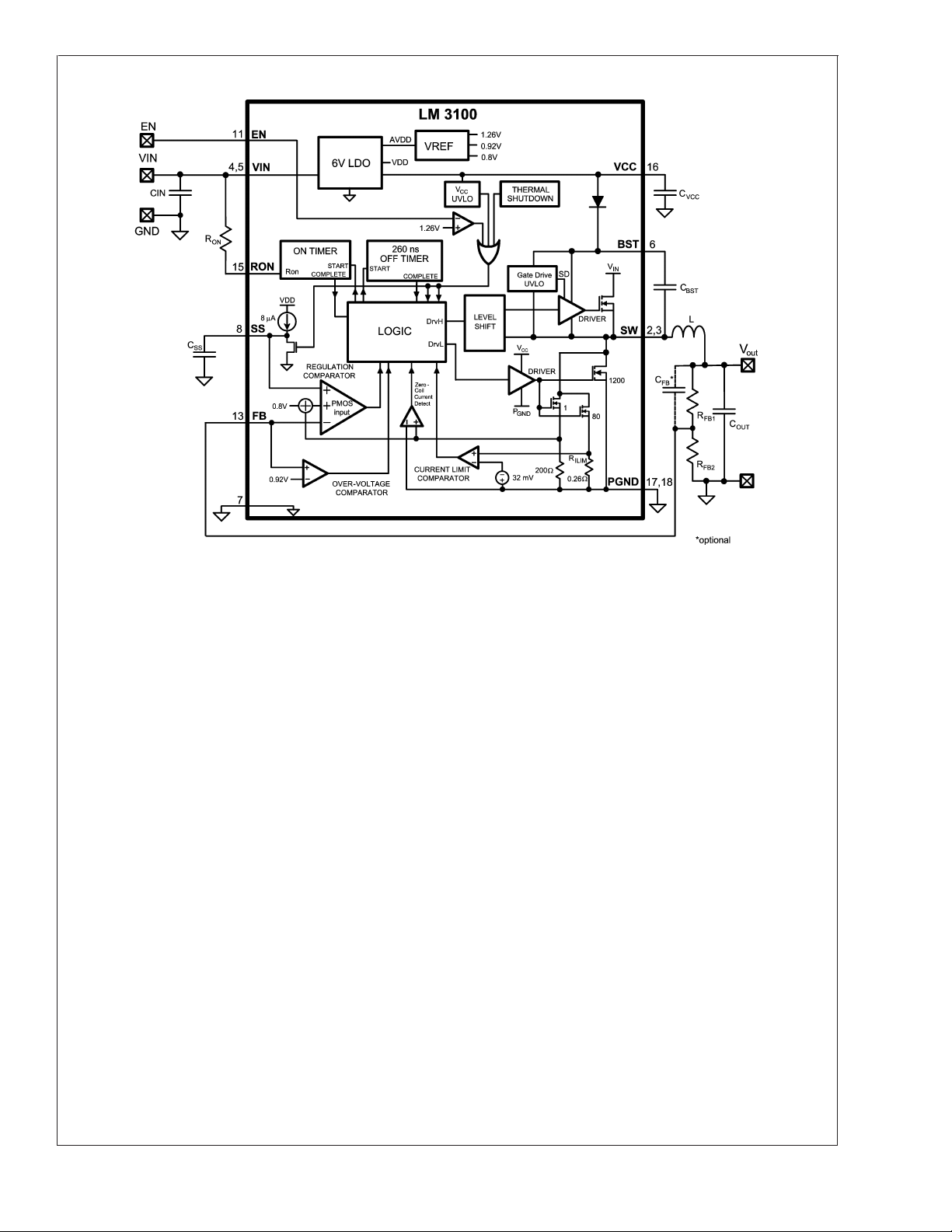
Simplified Functional Block Diagram
LM3100
20174701
www.national.com9
Functional Description
The LM3100 Step Down Switching Regulator features all
LM3100
functions needed to implement a cost effective, efficient buck
power converter capable of supplying 1.5A to a load. This
voltage regulator contains Dual 40V N-Channel buck synchronous switches and is available in a thermally enhanced
eTSSOP-20 package. The Constant ON-Time (COT) regulation scheme requires no loop compensation, results in fast
load transient response, and simplifies circuit implementation. It will work correctly even with an all ceramic output
capacitor network and does not rely on the output capacitor’s
ESR for stability. The operating frequency remains constant
with line and load variations due to the inverse relationship
between the input voltage and the on-time. The valley current limit detection circuit, internally set at 1.9A, inhibits the
high-side switch until the inductor current level subsides.
Please refer to the functional block diagram with a typical
application circuit.
The LM3100 can be applied in numerous applications and
can operate efficiently from inputs as high as 36V. Protection
features include: Thermal shutdown, V
CC
lockout, gate drive under-voltage lockout.
Hysteretic Control Circuit Overview
The LM3100 buck DC-DC regulator employs a control
scheme in which the high-side switch on-time varies inversely with the line voltage (V
comparator and the one-shot on-timer, with the output voltage feedback (FB) compared with an internal reference of
0.8V. If the FB level is below the reference the buck switch is
turned on for a fixed time determined by the input voltage
and a programming resistor (R
the switch remains off for a minimum of 260ns. If FB is below
the reference at that time the switch turns on again for
another on-time period. The switching will continue until
regulation is achieved.
The regulator will operate in discontinuous conduction mode
at light load currents, and continuous conduction mode with
heavy load current. In discontinuous conduction mode
(DCM), current through the output inductor starts at zero and
ramps up to a peak during the on-time, then ramps back to
zero before the end of the off-time. The next on-time period
starts when the voltage at FB falls below the internal reference. Until then the inductor current remains zero and the
load is supplied entirely by the output capacitor. In this mode
the operating frequency is lower than in continuous conduction mode, and varies with load current. Conversion efficiency is maintained since the switching losses are reduced
with the reduction in load and switching frequency. The
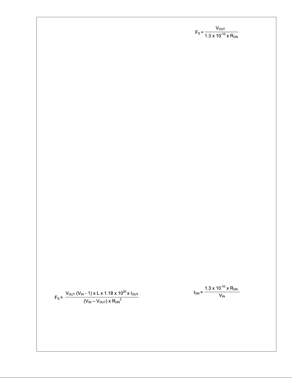
discontinuous operating frequency can be calculated approximately as follows:
). Control is based on a
IN
). Following the on-time,
ON
under-voltage
(2)
The output voltage is set by two external resistors (R
). The regulated output voltage is calculated as follows:
R
FB2
V
=0.8Vx(R
OUT
FB1+RFB2
)/R
FB2
FB1
(3)
Start-up Regulator (VCC)
The start-up regulator is integrated within LM3100. The input
pin (VIN) can be connected directly to line voltage up to 36V,
with transient capability to 40V. The V
output regulates at
CC
6V, and is current limited to 65 mA. Upon power up, the
regulator sources current into the external capacitor at V
(C
VCC
). C
must be at least 680nF for stability. When the
VCC
CC
voltage on the VCC pin reaches the under-voltage lockout
threshold of 3.75V, the buck switch is enabled and the
Soft-start pin is released to allow the soft-start capacitor
) to charge.
(C
SS
The minimum input voltage is determined by the dropout
voltage of V
V). If VIN is less than )4.0V, the V
, and the VCCUVLO falling threshold ()3.7
CC
UVLO activates to shut
CC
off the output.
Regulation Comparator
The feedback voltage at FB is compared to the internal
reference voltage of 0.8V. In normal operation (the output
voltage is regulated), an on-time period is initiated when the
voltage at FB falls below 0.8V. The buck switch stays on for
the on-time, causing the FB voltage to rise above 0.8V. After
the on-time period, the buck switch stays off until the FB
voltage falls below 0.8V. Bias current at the FB pin is nominally 100 nA.
Over-Voltage Comparator
The voltage at FB is compared to an internal 0.92V reference. If the voltage at FB rises above 0.92V the on-time
pulse is immediately terminated. This condition can occur if
the input voltage, or the output load, changes suddenly.
Once the OVP is activated, the buck switch remains off until
the voltage at FB pin falls below 0.92V. The low side switch
will stay on to discharge the inductor energy and until the
inductor current decays to zero. The low side switch will be
turned off.
ON-Time Timer, Shutdown
The LM3100 main switch is determined by the RONresistor
and the input voltage (V
), and is calculated from:
IN
,
(1)
where R
= the load resistance
L
In continuous conduction mode (CCM), current always flows
through the inductor and never reaches zero during the
off-time. In this mode, the operating frequency remains relatively constant with load and line variations. The CCM operating frequency can be calculated approximately as follows:
www.national.com 10
(4)
The inverse relationship with VIN results in a nearly constant
frequency as V
minimum on-time (at maximum V
is varied. RONshould be selected for a
IN
) greater than 200 ns for
IN
proper current limit operation. This requirement limits the
maximum frequency for each application, depending on V
and V
, calculated from the following:
OUT
IN
ON-Time Timer, Shutdown (Continued)
(5)
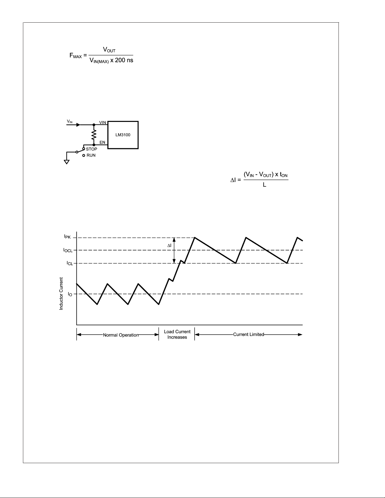
The LM3100 can be remotely shut down by taking the EN pin
below 1.1V. Refer to Figure 1. In this mode the SS pin is
internally grounded, the on-timer is disabled, and bias currents are reduced. Releasing the EN pin allows normal
operation to resume. The voltage at the EN pin is between
1.5V and 3.0V, depending on V
and the pull-up resistor.
IN
20174704
FIGURE 1. Shutdown Implementation
Current Limit
Current limit detection occurs during the off-time by monitoring the re-circulating current through the low-side synchro-
nous switch. Referring to Functional Block Diagram, when
the buck switch is turned off, inductor current flows through
the load, into PGND, and through the internal low-side synchronous switch. If that current exceeds 1.9A the current
limit comparator toggles, forcing a delay to the start of the
next on-time period. The next cycle starts when the recirculating current falls back below 1.9A and the voltage at
FB is below 0.8V. The inductor current is monitored during
the low-side switch on-time. As long as the overload condition persists and the inductor current exceeds 1.9A, the
high-side switch will remain inhibited. The operating frequency is lower during an over-current due to longer than
normal off-times.
Figure 2 illustrates the inductor current waveform. During
normal operation the load current is low, the average of the
ripple waveform. When an overload occurs the current ratchets up until it exceeds 1.9A. During the Current Limited
portion of Figure 2, the current ramps down to 1.9A during
each off-time, initiating the next on-time (assuming the volt-
<
age at FB is
0.8V). During each on-time the current ramps
up an amount equal to:
(6)
During this time the LM3100 is in a constant current mode,
with an average load current (I
) equal to 1.9A +∆I/2.
OCL
LM3100
FIGURE 2. Inductor Current - Current Limit Operation
20174705
www.national.com11

N - Channel Buck Switch and Driver
LM3100
The LM3100 integrates an N-Channel buck (high-side)
switch and associated floating high voltage gate driver. The
gate drive circuit works in conjunction with an external bootstrap capacitor and an internal high voltage diode. A 33 nF
capacitor (C
) connected between BST and SW pins pro-
BST
vides voltage to the high-side driver during the buck switch
on-time. During each off-time, the SW pin falls to approximately -1V and C
charges from the VCCsupply through
BST
the internal diode. The minimum off-time of 260ns ensures
adequate time each cycle to recharge the bootstrap capacitor.
Softstart
The soft-start feature allows the converter to gradually reach
a steady state operating point, thereby reducing start-up
stresses and current surges. Upon turn-on, after V
reaches the under-voltage threshold, an internal 8µA current
source charges up the external capacitor at the SS pin. The
ramping voltage at SS (and the non-inverting input of the
regulation comparator) ramps up the output voltage in a
controlled manner.
An internal switch grounds the SS pin if V
under-voltage lockout threshold, if a thermal shutdown occurs, or if the EN pin is grounded. Using an externally
controlled switch, the output voltage can be shut off by taking
the SS pin to ground. Releasing the switch allows the SS pin
to ramp up, and the output voltage to return to normal. The
shut-down configuration is shown in Figure 3.
CC
CC
is below the
R
FB1/RFB2
and R
R
FB1
should be chosen from standard value resis-
FB2
=(V
OUT
/0.8V) - 1
tors in the range of 1.0 kΩ -10kΩ which satisfy the above
ratio.
For V
= 0.8V, the FB pin can be connected to the output
OUT
directly. However, the converter operation needs a minimum
inductor current ripple to maintain good regulation when no
load is connected. This minimum load is about 10 µA and
can be implemented by adding a pre-load resistor to the
output.
: The minimum value for RON is calculated from:
R
ON
Equation 1 can be used to select RONif a specific frequency
is desired as long as the above limitation is met.
L: The main parameter effected by the inductor is the output
current ripple amplitude (I
). The maximum allowable (I
OR
OR
must be determined at both the minimum and maximum
nominal load currents. At minimum load current, the lower
peak must not reach 0 mA. At maximum load current, the
upper peak must not exceed the current limit threshold
(1.9A). The allowable ripple current is calculated from the
following equations:
I
OR(MAX1)
=2xI
O(min)
or
I
OR(MAX2)
= 2 x (1.9A - I
O(max)
)
20174706
FIGURE 3. Alternate Shutdown Implementation
Thermal Protection
The LM3100 should be operated so the junction temperature
does not exceed the maximum limit. An internal Thermal
Shutdown circuit, which activates (typically) at 165˚C, takes
the controller to a low power reset state by disabling the buck
switch and the on-timer, and grounding the Softstart pin. This
feature helps prevent catastrophic failures from accidental
device overheating. When the junction temperature falls
back below 145˚C (typical hysteresis = 20˚C), the Softstart
pin is released and normal operation resumes.
Applications Information
EXTERNAL COMPONENTS
The following guidelines can be used to select the external
components.
R
FB1
from:
and R
: The ratio of these resistors is calculated
FB2
The lesser of the two ripple amplitudes calculated above is
then used in the following equation:
(7)
where V
is the maximum input voltage and Fs is deter-
IN
mined from equation 1. This provides a value for L. The next
larger standard value should be used. L should be rated for
current level shown in Figure 2.
the I
PK
Inductor Selector for V
OUT
= 3.3V
20174736
www.national.com 12

Applications Information (Continued)
Inductor Selector for V
OUT
= 0.8V
C
: The recommended value for CBST is 33 nF. A high
BST
quality ceramic capacitor with low ESR is recommended as
supplies a surge current to charge the buck switch gate
C
BST
at turn-on. A low ESR also helps ensure a complete recharge
during each off-time.
: The capacitor at the SS pin determines the soft-start
C
SS
time, i.e. the time for the reference voltage at the regulation
comparator, and the output voltage, to reach their final value.
The time is determined from the following:
CFB: If output voltage is higher than 1.6V, this feedback cap
is needed for Discontinuous Conduction Mode to improve
the output ripple performance, the recommended value for
is 10 nF.
C
FB
LM3100
20174737
C
: The capacitor on the VCCoutput provides not only
VCC
noise filtering and stability, but also prevents false triggering
of the V
this reason, C
UVLO at the buck switch on/off transitions. For
CC
should be no smaller than 680 nF for
VCC
stability, and should be a good quality, low ESR, ceramic
capacitor.
and CO3: COshould generally be no smaller than 10 µF.
C
O
Experimentation is usually necessary to determine the minimum value for C
, as the nature of the load may require a
O
larger value. A load which creates significant transients requires a larger value for C
is a small value ceramic capacitor to further suppress
C
O3
high frequency noise at V
than a fixed load.
O
. A 47nF is recommended,
OUT
located close to the LM3100.
and C
C
IN
current during the on-time, and limit the voltage ripple at V
on the assumption that the voltage source feeding V
: CIN’s purpose is to supply most of the switch
IN3
IN
has
IN
an output impedance greater than zero. If the source’s dynamic impedance is high (effectively a current source), it
supplies the average input current, but not the ripple current.
At maximum load current, when the buck switch turns on, the
current into V
suddenly increases to the lower peak of the
IN
inductor’s ripple current, ramps up to the peak value, then
drop to zero at turn-off. The average current during the
on-time is the load current. For a worst case calculation, C
must supply this average load current during the maximum
on-time. C
is calculated from:
IN
(8)
where I
and ∆V is the allowable ripple voltage at V
C
IN3
long lead inductance at V
is the load current, tONis the maximum on-time,
O
.
IN
’s purpose is to help avoid transients and ringing due to
. A low ESR, 0.1µF ceramic chip
IN
capacitor is recommended, located close to the LM3100.
PC BOARD LAYOUT
The LM3100 regulation, over-voltage, and current limit comparators are very fast, and will respond to short duration
noise pulses. Layout considerations are therefore critical for
optimum performance. The layout must be as neat and
compact as possible, and all of the components must be as
close as possible to their associated pins. Refer to the
functional block diagram, the loop formed by C
, the high
IN
and low-side switches internal to the IC, and the PGND pin
should be as small as possible. The PGND connection to Cin
should be as short and direct as possible. There should be
several vias connecting the Cin ground terminal to the
ground plane placed as close to the capacitor as possible.
The boost capacitor should be connected as close to the SW
and BST pins as possible. The feedback divider resistors
and the C
capacitor should be located close to the FB pin.
FB
A long trace run from the top of the divider to the output is
,
generally acceptable since this is a low impedance node.
Ground the bottom of the divider directly to the GND (pin 7).
The output capacitor, C
, should be connected close to
OUT
the load and tied directly into the ground plane. The inductor
should connect close to the SW pin with as short a trace as
possible to help reduce the potential for EMI (electromagnetic interference) generation.
If it is expected that the internal dissipation of the LM3100
will produce excessive junction temperatures during normal
IN
operation, good use of the PC board’s ground plane can help
considerably to dissipate heat. The exposed pad on the
bottom of the IC package can be soldered to a ground plane
and that plane should extend out from beneath the IC to help
dissipate the heat. The exposed pad is internally connected
to the IC substrate. Additionally the use of wide PC board
traces, where possible, can help conduct heat away from the
IC. Using numerous vias to connect the die attach pad to an
internal ground plane is a good practice. Judicious positioning of the PC board within the end product, along with the
use of any available air flow (forced or natural convection)
can help reduce the junction temperature.
www.national.com13

Applications Information (Continued)
LM3100
Typical Application Schematic for V
Typical Application Schematic for V
OUT
OUT
= 3.3V
20174716
20174717
= 0.8V
www.national.com 14

Physical Dimensions inches (millimeters) unless otherwise noted
LM3100 SIMPLE SWITCHER
®
Synchronous 1MHz 1.5A Step-Down Voltage Regulator
20-Lead Plastic eTSSOP Package
NS Package Number MXA20A
National does not assume any responsibility for use of any circuitry described, no circuit patent licenses are implied and National reserves
the right at any time without notice to change said circuitry and specifications.
For the most current product information visit us at www.national.com.
LIFE SUPPORT POLICY
NATIONAL’S PRODUCTS ARE NOT AUTHORIZED FOR USE AS CRITICAL COMPONENTS IN LIFE SUPPORT DEVICES OR SYSTEMS
WITHOUT THE EXPRESS WRITTEN APPROVAL OF THE PRESIDENT AND GENERAL COUNSEL OF NATIONAL SEMICONDUCTOR
CORPORATION. As used herein:
1. Life support devices or systems are devices or systems
which, (a) are intended for surgical implant into the body, or
(b) support or sustain life, and whose failure to perform when
properly used in accordance with instructions for use
2. A critical component is any component of a life support
device or system whose failure to perform can be reasonably
expected to cause the failure of the life support device or
system, or to affect its safety or effectiveness.
provided in the labeling, can be reasonably expected to result
in a significant injury to the user.
BANNED SUBSTANCE COMPLIANCE
National Semiconductor follows the provisions of the Product Stewardship Guide for Customers (CSP-9-111C2) and Banned Substances
and Materials of Interest Specification (CSP-9-111S2) for regulatory environmental compliance. Details may be found at:
www.national.com/quality/green.
Lead free products are RoHS compliant.
National Semiconductor
Americas Customer
Support Center
Email: new.feedback@nsc.com
Tel: 1-800-272-9959
www.national.com
National Semiconductor
Europe Customer Support Center
Fax: +49 (0) 180-530 85 86
Email: europe.support@nsc.com
Deutsch Tel: +49 (0) 69 9508 6208
English Tel: +44 (0) 870 24 0 2171
Français Tel: +33 (0) 1 41 91 8790
National Semiconductor
Asia Pacific Customer
Support Center
Email: ap.support@nsc.com
National Semiconductor
Japan Customer Support Center
Fax: 81-3-5639-7507
Email: jpn.feedback@nsc.com
Tel: 81-3-5639-7560
 Loading...