

NSC LM307H, LM107H, LM307N Datasheet
LM107/LM207/LM307 Operational Amplifiers
General Description
The LM107 series are complete, general purpose operational amplifiers, with the necessary frequency compensation
built into the chip. Advanced processing techniques make
the input currents a factor of ten lower than industry standards like the 709. Yet, they are a direct, plug-in replacement for the 709, LM101A and 741.
The LM107 series offers the features of the LM101A, which
makes its application nearly foolproof. In addition, the device provides better accuracy and lower noise in high impedance circuitry. The low input currents also make it particularly well suited for long interval integrators or timers, sample and hold circuits and low frequency waveform genera-
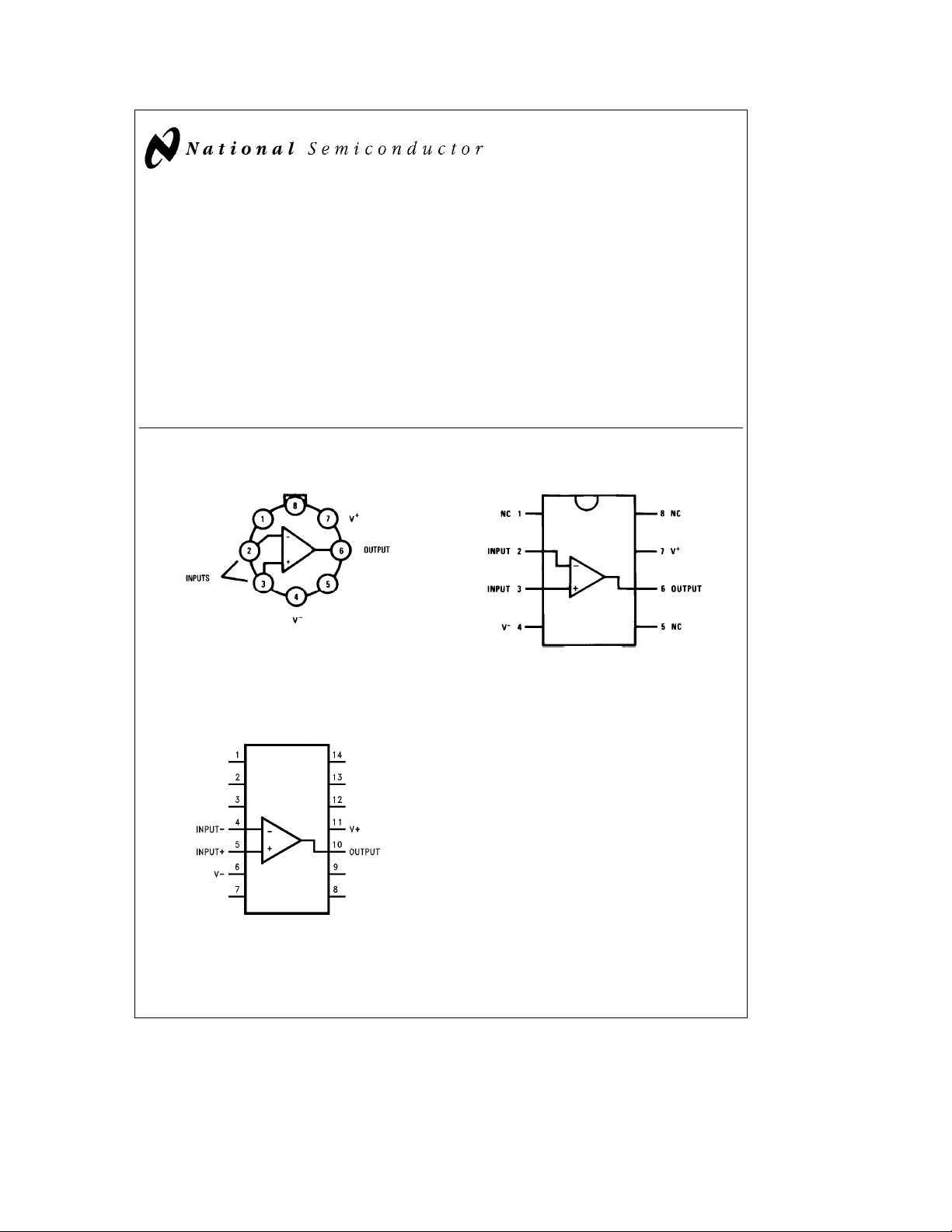
Connection Diagrams
Metal Can Package
tors. Further, replacing circuits where matched transistor
pairs buffer the inputs of conventional IC op amps, it can
give lower offset voltage and drift at a lower cost.
The LM107 is guaranteed over a
ature range, the LM207 from
LM307 from 0
Ctoa70§C.
§
Features
Y
Offset voltage 3 mV maximum over temperature
Y
Input current 100 nA maximum over temperature
Y
Offset current 20 nA maximum over temperature
Y
Guaranteed drift characteristics
Dual-in-Line Package
December 1994
b
55§Ctoa125§C temper-
b
25§Ctoa85§C and the
LM107/LM207/LM307 Operational Amplifiers
Note: Pin 4 connected to case.
Top View
Order Number LM107H/883*
See NS Package Number H08C
Dual-in-Line Package
TL/H/7757– 2
TL/H/7757– 3
Top View
Order Number LM107J/883* or LM207J
See NS Package Number J08A
Order Number LM307N
See NS Package Number N08A
TL/H/7757– 13
Order Number LM107J-14/883*
See NS Package Number J14A
*Available per SMDÝ5962-8958901.
C
1995 National Semiconductor Corporation RRD-B30M115/Printed in U. S. A.
TL/H/7757
Absolute Maximum Ratings
If Military/Aerospace specified devices are required, please contact the National Semiconductor Sales Office/
Distributors for availability and specifications.
(Note 4)
LM107/LM207 LM307
Supply Voltage
g
22V
Power Dissipation (Note 1) 500 mW 500 mW
Differential Input Voltage
Input Voltage (Note 2)
g
30V
g
15V
Output Short Circuit Duration Continuous Continuous LM307 0
Operating Temperature Range (T
(LM107)
(LM207)
Storage Temperature Range
Lead Temperature (Soldering, 10 sec) 260
) ESD rating to be determined.
A
b
55§Ctoa125§C0
b
25§Ctoa85§C
b
65§Ctoa150§C
C 260§C
§
g
18V
g
30V LM107
g
15V LM207
Ctoa70§C
§
b
65§Ctoa150§C
b
b
T
MIN
55§C
25§C
C
§
a
a
a
T
MAX
125§C
85§C
70§C
Electrical Characteristics (Note 3)
Parameter Conditions
Input Offset Voltage T
Input Offset Current T
Input Bias Current T
Input Resistance T
Supply Current T
Large Signal Voltage T
Gain V
Input Offset Voltage R
V
V
A
A
A
A
A
S
S
A
OUT
S
e
e
e
e
e
e
e
e
s
s
25§C, R
50 kX 0.7 2.0 2.0 7.5 mV
S
25§C 1.5 10 3.0 50 nA
25§C 30 75 70 250 nA
25§C 1.5 4.0 0.5 2.0 MX
25§C
g
20V 1.8 3.0 mA
g
15V 1.8 3.0 mA
e
g
10V, R
g
15V
S
t
2kX
L
25§C, V
e
50 kX 3.0 10 mV
Average Temperature
Coefficient of Input 3.0 15 6.0 30 mV/§C
Offset Voltage
Input Offset Current 20 70 nA
Average Temperature 25§CsT
Coefficient of Input T
Offset Current
MIN
s
T
A
MAX
s
s
T
25§C 0.02 0.2 0.02 0.6 nA/§C
A
Input Bias Current 100 300 nA
Supply Current T
A
ea
125§C, V
e
g
20V 1.2 2.5 mA
S
LM107/LM207 LM307
Units
Min Typ Max Min Typ Max
50 160 25 160 V/mV
0.01 0.1 0.01 0.3 nA/§C
2
Electrical Characteristics (Note 3) (Continued)
Parameter Conditions
e
Large Signal Voltage V
Gain R
Output Voltage Swing V
Input Voltage Range V
Common Mode R
Rejection Ratio
Supply Voltage R
Rejection Ratio
Note 1: The maximum junction temperature of the LM107 is 150§C, and the LM207/LM307 is 100§C. For operating at elevated temperatures, devices in the H08
package must be derated based on a thermal resistance of 165
package is 100
Note 2: For supply voltages less than
Note 3: These specifications apply for
a
70§C andg5VsV
Note 4: Refer to RETS107X for LM107H and LM107J military specifications.
C/W, junction to ambient.
§
s
g
15V for the LM307 unless otherwise specified.
S
g
15V, V
S
t
2kX 25 V/mV
L
e
g
15V
S
e
R
10 kX
L
e
R
2kX
L
e
g
20V
S
e
g
V
15V
S
s
50 kX
S
s
50 kX
S
g
15V, the absolute maximum input voltage is equal to the supply voltage.
g
5VsV
e
OUT
s
a
20V andb55§CsT
S
g
10V 15
C/W, junction to ambient, or 30§C/W, junction to case. The thermal resistance of the dual-in-line
§
LM107/LM207 LM307
Min Typ Max Min Typ Max
g
g
g
g
12
10
14
g
13
g
g
g
12
10
14 V
g
13 V
15 V
a
15
b
13
g
a
12
15 V
b
13
80 96 70 90 dB
80 96 70 96 dB
s
a
125§C for the LM107 orb25§CsT
A
a
85§C for the LM207, and 0§CsT
A
Units
A
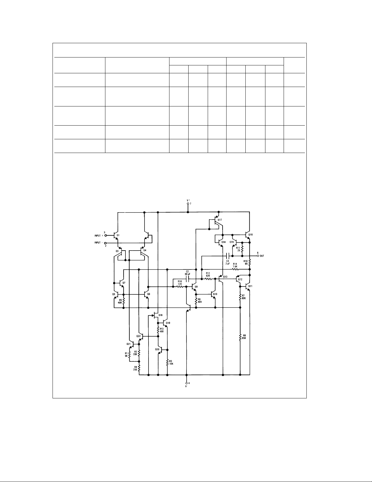
Schematic Diagram*
s
*Pin connections shown are for metal can. TL/H/7757– 1
3
 Loading...