

NSC LM305AH, LM305H Datasheet
LM105/LM305/LM305A
Voltage Regulators
General Description
The LM105 series are positive voltage regulators similar to
the LM100, except that an extra gain stage has been added
for improved regulation. Aredesignofthe biasing circuitry removes any minimum load current requirement and at the
same time reduces standby current drain, permitting higher
voltage operation. They are direct, plug-in replacements for
the LM100 in both linear and switching regulator circuits with
output voltages greater than 4.5V. Important characteristics
of the circuits are:
Output voltage adjustable from 4.5V to 40V
•
Output currents in excess of 10A possible by adding ex-
•
ternal transistors
Load regulation better than 0.1%, full load with current
•
limiting
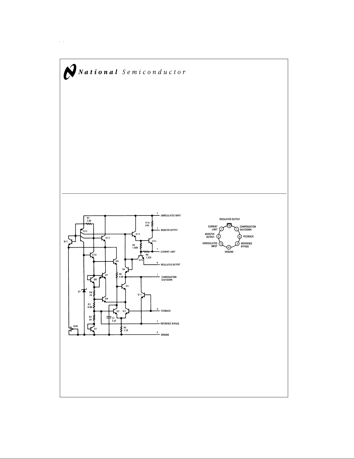
Schematic and Connection Diagrams
June 1999
DC line regulation guaranteed at 0.03%/V
•
Ripple rejection on 0.01%V
•
45 mA output current without external pass transistor
•
(LM305A)
Like the LM100, they also feature fast response to both load
and line transients, freedom from oscillations with varying resistive and reactive loads and the ability to start reliably on
any load within rating. The circuits are built on a single silicon
chip and are supplied in a TO-99 metal can.
The LM105 is specified for operation for −55˚C ≤ T
+125˚C, and the LM305/LM305A is specified for 0˚C ≤ T
+70˚C.
Metal Can Package
A
A
LM105/LM305/LM305A Voltage Regulators
≤
≤
DS007755-3
Order Number LM105H, LM105H/883,
#
SMD
5962-8958801, LM305H or LM305AH
See NS Package Number H08C
DS007755-1
© 1999 National Semiconductor Corporation DS007755 www.national.com
Top View
Absolute Maximum Ratings (Note 1)
If Military/Aerospace specified devices are required,
please contact the National Semiconductor Sales Office/
Distributors for availability and specifications.
(Note 5)
LM105 LM305 LM305A
Input Voltage 50V 40V 50V
Input-Output Differential 40V 40V 40V
Power Dissipation (Note 1) 800 mW 800 mW 800 mW
Operating Temperature Range −55˚C to +125˚C 0˚C to +70˚C 0˚C to +70˚C
Storage Temperature Range −65˚C to +150˚C 65˚C to +150˚C −65˚C to +150˚C
Lead Temperature (Soldering, 10 seconds) 300˚C 300˚C 300˚C
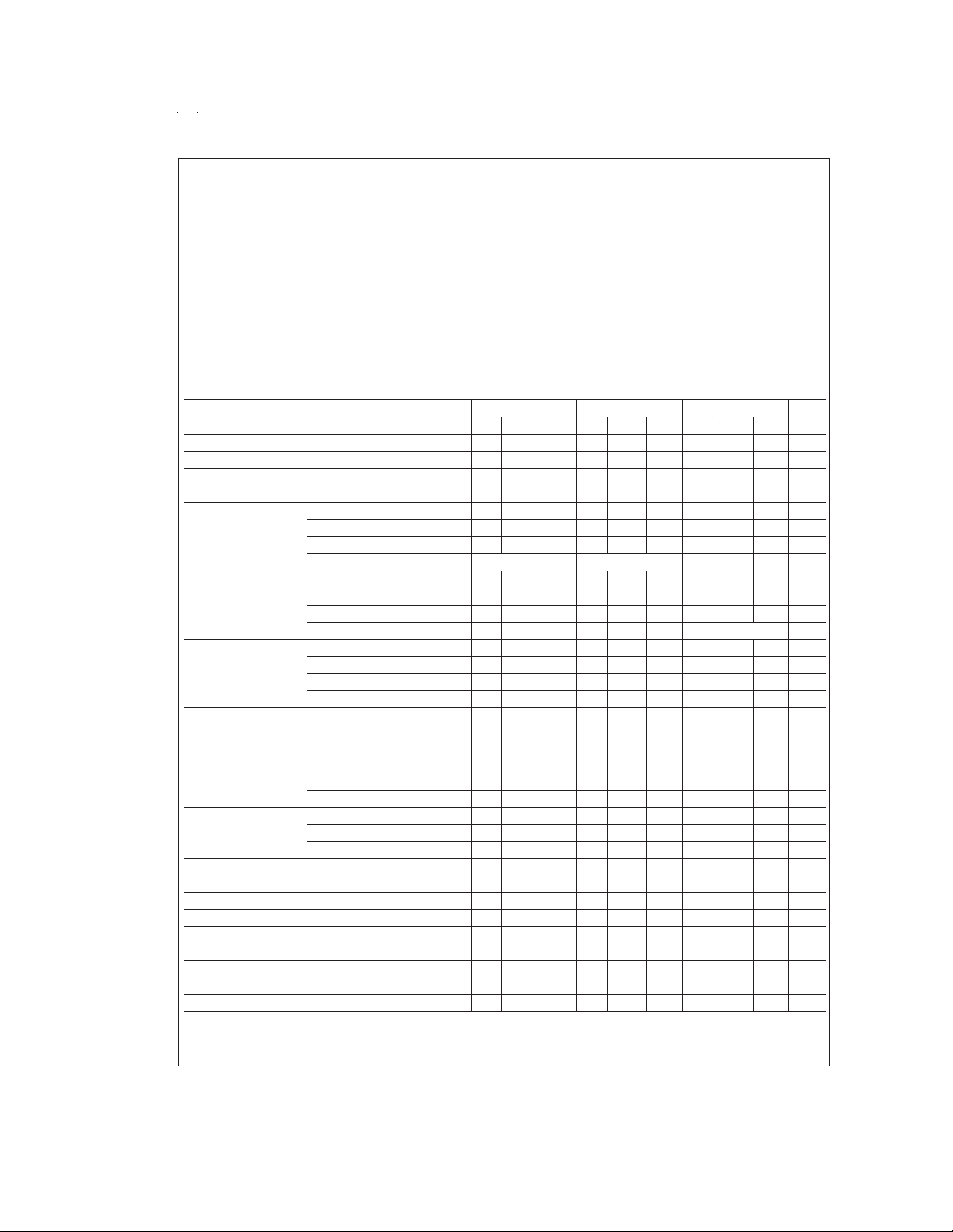
Electrical Characteristics (Note 2)
Parameter Conditions LM105 LM305 LM305A Units
Min Typ Max Min Typ Max Min Typ Max
Input Voltage Range 8.5 50 8.5 40 8.5 50 V
Output Voltage Range 4.5 40 4.5 30 4.5 40 V
Input-Output Voltage 3.0 30 3.0 30 3.0 30 V
Differential
Load Regulation R
(Note 3) R
Line Regulation T
=
SC
=
SC
=
R
SC
=
R
SC
=
R
SC
=
R
SC
=
25˚C
A
0˚C ≤ T
V
IN−VOUT
V
Temperature Stability T
IN−VOUT
A(MIN)
Feedback Sense
Voltage
Output Noise Voltage 10 Hz ≤ f ≤ 10 kHz
=
C
REF
=
C
REF
Standby Current Drain V
Current Limit T
Sense Voltage V
=
30V, T
IN
=
V
40V 0.8 2.0 mA
IN
=
V
50V 0.8 2.0 0.8 2.0 mA
IN
=
25˚C, R
A
=
OUT
Long Term Stability 0.1 0.1 0.1
Ripple Rejection C
θ
JA
=
REF
TO-99 Board Mount 230 230 230 ˚C/W
in Still Air
θ
JA
TO-99 Board Mount in 92 92 92 ˚C/W
400 LF/Min Air Flow
θ
JC
TO-99 25 25 25 ˚C/W
=
10Ω,T
10Ω,T
10Ω,T
0Ω,T
0Ω,T
0Ω,T
A
≤ TA≤ T
25˚C 0.02 0.05 0.02 0.05
A
=
T
A
A(MAX)
=
T
A
A(MIN)
=
25˚C 0.02 0.2
A
=
70˚C 0.03 0.4
A
=
0˚C 0.03 0.4
A
0.03 0.1 0.03 0.1
0.03 0.1 0.03 0.1
0 ≤ I
≤ 12 mA 0 ≤ IO≤ 12 mA
O
≤ +70˚C
=
≤ 5V, T
≥ 5V, T
25˚C 0.025 0.06 0.025 0.06 0.025 0.06%/V
A
=
25˚C 0.015 0.03 0.015 0.03 0.015 0.03%/V
A
A(MAX)
0.3 1.0 0.3 1.0 0.3 1.0
0 ≤ I
O
1.63 1.7 1.81 1.63 1.7 1.81 1.55 1.7 1.85 V
0 0.005 0.005 0.005
0.1 µF 0.002 0.002 0.002
=
25˚C mA
A
=
10Ω, 225 300 375 225 300 375 225 300 375 mV
SC
0V, (Note 4)
10 µF, f=120 Hz 0.003 0.003 0.003
≤ 45 mA
%
%
%
%
%
%
%
%
%
/V
/V
%
%
%
%
/V
www.national.com 2
Electrical Characteristics (Note 2) (Continued)
Note 1: The maximum junction temperature of the LM105 and LM305A is 150˚C, and the LM305 is 85˚C. For operation at elevated temperatures, devices in the
H08C package must be derated based on a thermal resistance of 168˚C/W junction to ambient, or 25˚C/W junction to case. Peak dissipations to 1W are allowable
providing the dissipation rating is not exceeded with the power average over a five second interval for the LM105 and averaged over a two second interval for the
LM305.
Note 2: Unless otherwise specified, these specifications apply for temperatures within the operating temperature range, for input and output voltages within the
range given, andfora divider impedance seen by the feedback terminal of 2 kΩ. Load and line regulation specifications are for a constant junction temperature. Temperature drift effects must be taken into account separately when the unit is operating under conditions of high dissipation.
Note 3: The output currents given, as well as the load regulation, can be increased by the addition of external transistors. The improvement factor will be roughly
equal to the composite current gain of the added transistors.
Note 4: With no external pass transistor.
Note 5: Refer to RETS105X Drawing for military specifications for the LM105.
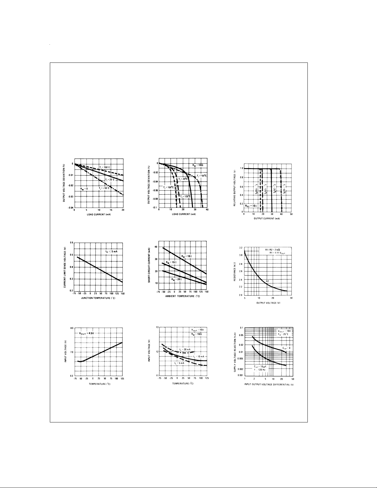
Typical Performance Characteristics
Load Regulation
Current Limit Sense Voltage
DS007755-18
Minimum Input Voltage
DS007755-15
Load Regulation
Short Circuit Current
Regulator Dropout Voltage
DS007755-16
DS007755-19
Current Limiting
Characteristics
DS007755-17
Optimum Divider Resistance
Values
DS007755-20
Supply Voltage Rejection
DS007755-21
DS007755-22
DS007755-23
www.national.com3
 Loading...