NSC LM302H Datasheet

TL/H/7753
LM102/LM302 Voltage Followers
November 1994
LM102/LM302 Voltage Followers
General Description
The LM102 series are high-gain operational amplifiers designed specifically for unity-gain voltage follower applications. Built on a single silicon chip, the devices incorporate
advanced processing techniques to obtain very low input
current and high input impedance. Further, the input transistors are operated at zero collector-base voltage to virtually
eliminate high temperature leakage currents. It can therefore be operated in a temperature stabilized component
oven to get extremely low input currents and low offset voltage drift.
The LM102, which is designed to operate with supply voltages between
g
12V andg15V, also features low input
capacitance as well as excellent small signal and large signal frequency responseÐall of which minimize high fre-
quency gain error. Because of the low wiring capacitances
inherent in monolithic construction, this fast operation can
be realized without increasing power consumption.
Features
Y
Fast slewing Ð 10V/ms
Y
Low input current Ð 10 nA (max)
Y
High input resistance Ð 10,000 MX
Y
No external frequency compensation required
Y
Simple offset balancing with optional 1 kX
potentiometer
Y
Plug-in replacement for both the LM101 and LM709 in
voltage follower applications
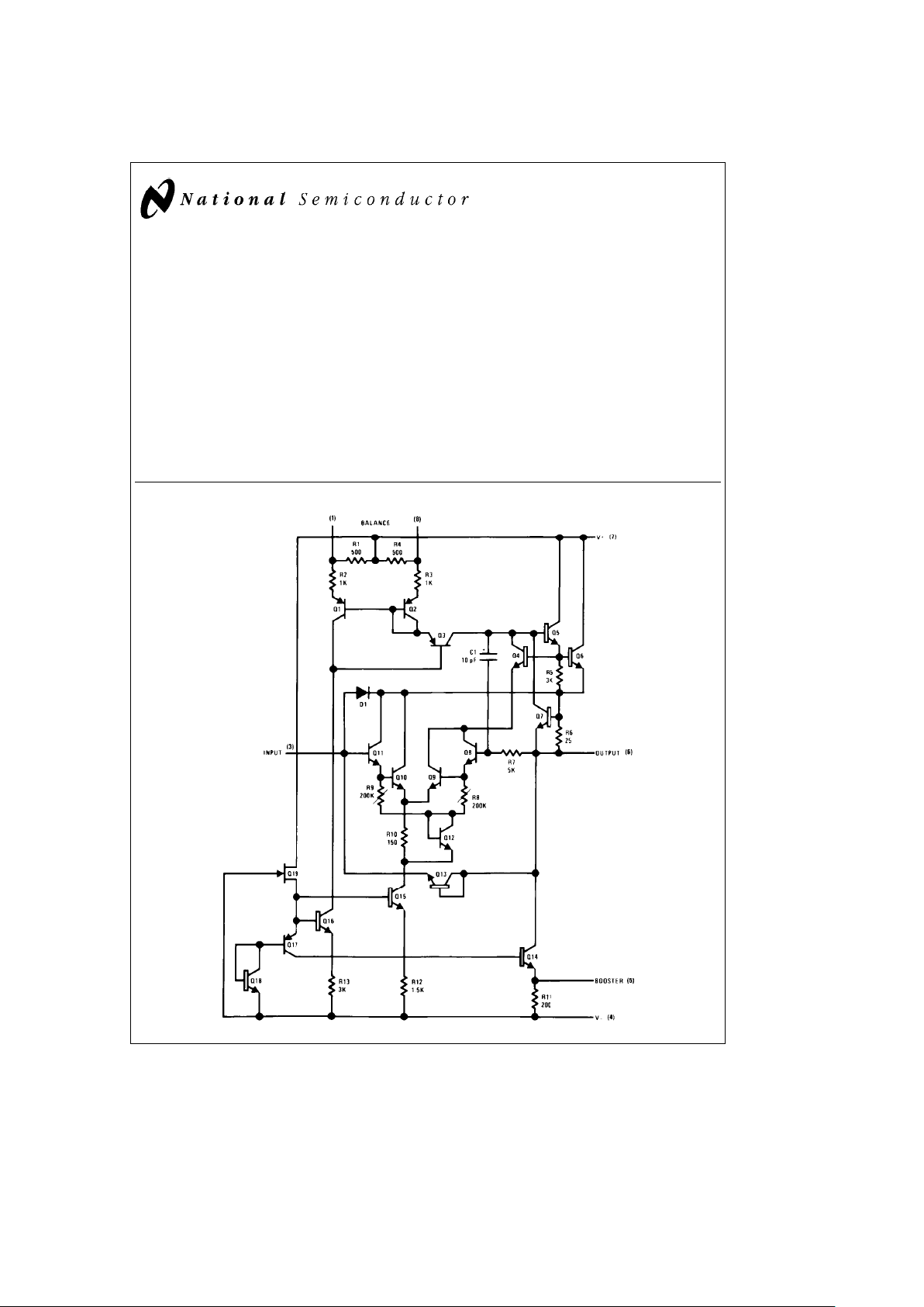
Schematic Diagram
TL/H/7753– 1
C
1995 National Semiconductor Corporation RRD-B30M115/Printed in U. S. A.

Absolute Maximum Ratings
If Military/Aerospace specified devices are required,
please contact the National Semiconductor Sales
Office/Distributors for availability and specifications.
(Note 6)
Supply Voltage
g
18V
Power Dissipation (Note 1) 500 mW
Input Voltage (Note 2)
g
15V
Output Short Circuit Duration (Note 3) Indefinite
Operating Free Air Temperature Range
LM102
b
55§Ctoa125§C
LM302 0
§
Ctoa70§C
Storage Temperature Range
b
65§Ctoa150§C
Lead Temperature (Soldering, 10 sec.) 300§C
ESD rating to be determined.
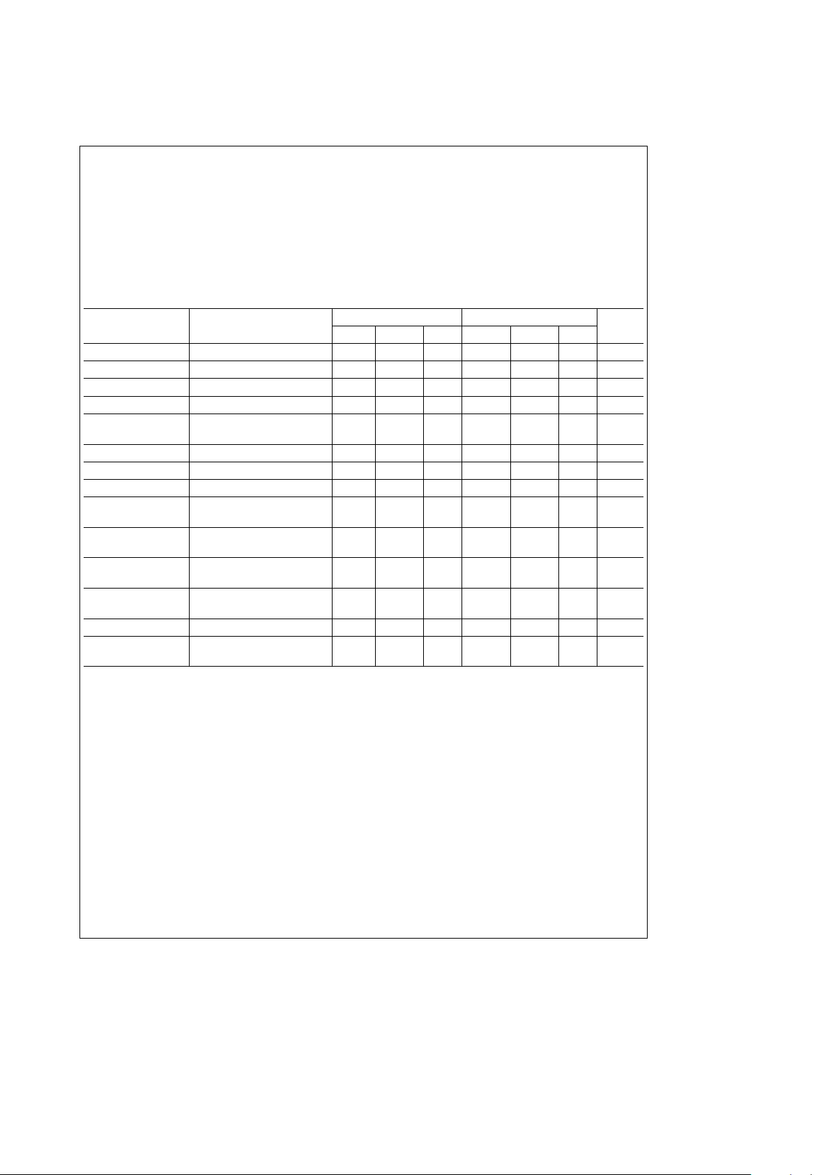
Electrical Characteristics (Note 4)
Parameter Conditions
LM102 LM302
Units
Min Typ Max Min Type Max
Input Offset Voltage T
A
e
25§C 2 5 5 15 mV
Input Bias Current T
A
e
25§C 3 10 10 30 nA
Input Resistance T
A
e
25§C10
10
10
12
10
9
10
12
X
Input Capacitance 3.0 3.0 pF
Large Signal Voltage T
A
e
25§C, V
S
g
15V,
0.999 0.9996 0.9985 0.9995 1.0 V/V
Gain V
OUT
e
g
10V, R
L
e
8kX
Output Resistance T
A
e
25§C 0.8 2.5 0.8 2.5 X
Supply Current T
A
e
25§C 3.5 5.5 3.5 5.5 mA
Input Offset Voltage 7.5 20 mV
Offset Voltage
620mV/
§
C
Temperature Drift
Input Bias Current T
A
e
TAMAX 3 10 3.0 15 nA
T
A
e
TAMIN 30 100 20 50 nA
Large Signal Voltage V
S
e
g
15V, V
OUT
e
g
10V,
0.999
Gain R
L
e
10 kX
Output Voltage V
S
e
g
15V, R
L
e
10 kX
g
10
g
10 V
Swing (Note 5)
Supply Current T
A
e
125§C 2.6 4.0 mA
Supply Voltage
g
12VsV
S
s
g
15V
60 60 dB
Rejection Ratio
Note 1: The maximum junction temperature of the LM102 is 150§C, while that of the LM302 is 85§C. For operating at elevated temperatures, devices in the H08
package must be derated based on a thermal resistance of 150
§
C/W, junction to ambient, or 20§C/W, junction to case.
Note 2: For supply voltages less than
g
15V, the absolute maximum input voltage is equal to the supply voltage.
Note 3: It is necessary to insert a resistor (at least 5k and preferably 10k) in series with the input pin when the amplifier is driven from low impedance sources to
prevent damage when the output is shorted and to ensure stability.
Note 4: These specifications apply for
g
12VsV
S
s
g
15V andb55§CsT
A
s
125§C for the LM102 and 0§CsT
A
s
70§C for the LM302 unless otherwise
specified.
Note 5: Increased output swing under load can be obtained by connecting an external resistor between the booster and V
b
terminals. See curve.
Note 6: Refer to RETS102X for the LM102H military specifications.
APPLICATION HINT
The input must be driven from a source impedance of typically 10 kX (5 kX Min) to maintain stability. The total source
impedance will be reduced at high frequencies if there is stray capacitance at the input pin. In these cases, a 10 kX resistor
should be inserted in series with the input, physically close to the input pin to minimize the stray capacitance and prevent
oscillation.
2
 Loading...