NSC LM2984CT Datasheet
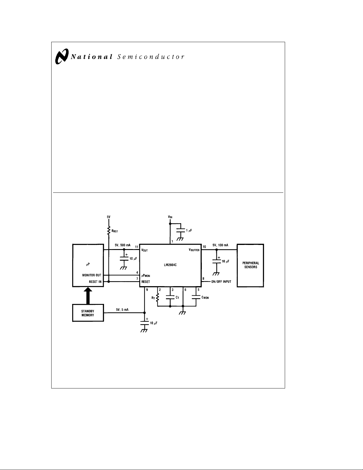
LM2984C Microprocessor Power Supply System
General Description
The LM2984C positive voltage regulator features three independent and tracking outputs capable of delivering the
power for logic circuits, peripheral sensors and standby
memory in a typical microprocessor system. The LM2984C
includes circuitry which monitors both its own high-current
output and also an external mP. If any error conditions are
sensed in either, a reset error flag is set and maintained until
the malfunction terminates. Since these functions are included in the same package with the three regulators, a
great saving in board space can be realized in the typical
microprocessor system. The LM2984C also features very
low dropout voltages on each of its three regulator outputs
(0.6V at the rated output current). Furthermore, the quiescent current can be reduced to 1 mA in the standby mode.
Designed also for vehicular applications, the LM2984C and
all regulated circuitry are protected from reverse battery installations or 2-battery jumps. Familiar regulator features
such as short circuit and thermal overload protection are
Typical Application Circuit
also provided. Fixed outputs of 5V are available in the plastic TO-220 power package.
Features
Y
Three low dropout tracking regulators
Y
Output current in excess of 500 mA
Y
Low quiescent current standby regulator
Y
Microprocessor malfunction RESET flag
Y
Delayed RESET on power-up
Y
Accurate pretrimmed 5V outputs
Y
Reverse battery protection
Y
Overvoltage protection
Y
Reverse transient protection
Y
Short circuit protection
Y
Internal thermal overload protection
Y
ON/OFF switch for high current outputs
Y
100% electrical burn-in in thermal limit
LM2984C
LM2984C Microprocessor Power Supply System
May 1989
C
must be at least 10 mFto
OUT
maintain stability. May be increased
without bound to maintain regulation
during transients. Locate as close as
possible to the regulator. This capac-
Order Number LM2984CT
See NS Package Number TA11B
C
1995 National Semiconductor Corporation RRD-B30M115/Printed in U. S. A.
TL/H/8821
itor must be rated over the same operating temperature range as the
regulator. The equivalent series resistance (ESR) of this capacitor is
critical; see curve.
TL/H/8821– 1
Absolute Maximum Ratings
If Military/Aerospace specified devices are required,
please contact the National Semiconductor Sales
Office/Distributors for availability and specifications.
Input Voltage
Survival Voltage (
k
100 ms) 35V
Operational Voltage 26V
Internal Power Dissipation Internally Limited
Operating Temperature Range (T
)0
A
Ctoa125§C
§
Maximum Junction Temperature (Note 1) 150§C
Storage Temperature Range
b
65§Ctoa150§C
Lead Temperature (Soldering, 10 sec.) 230§C
ESD rating is to be determined.
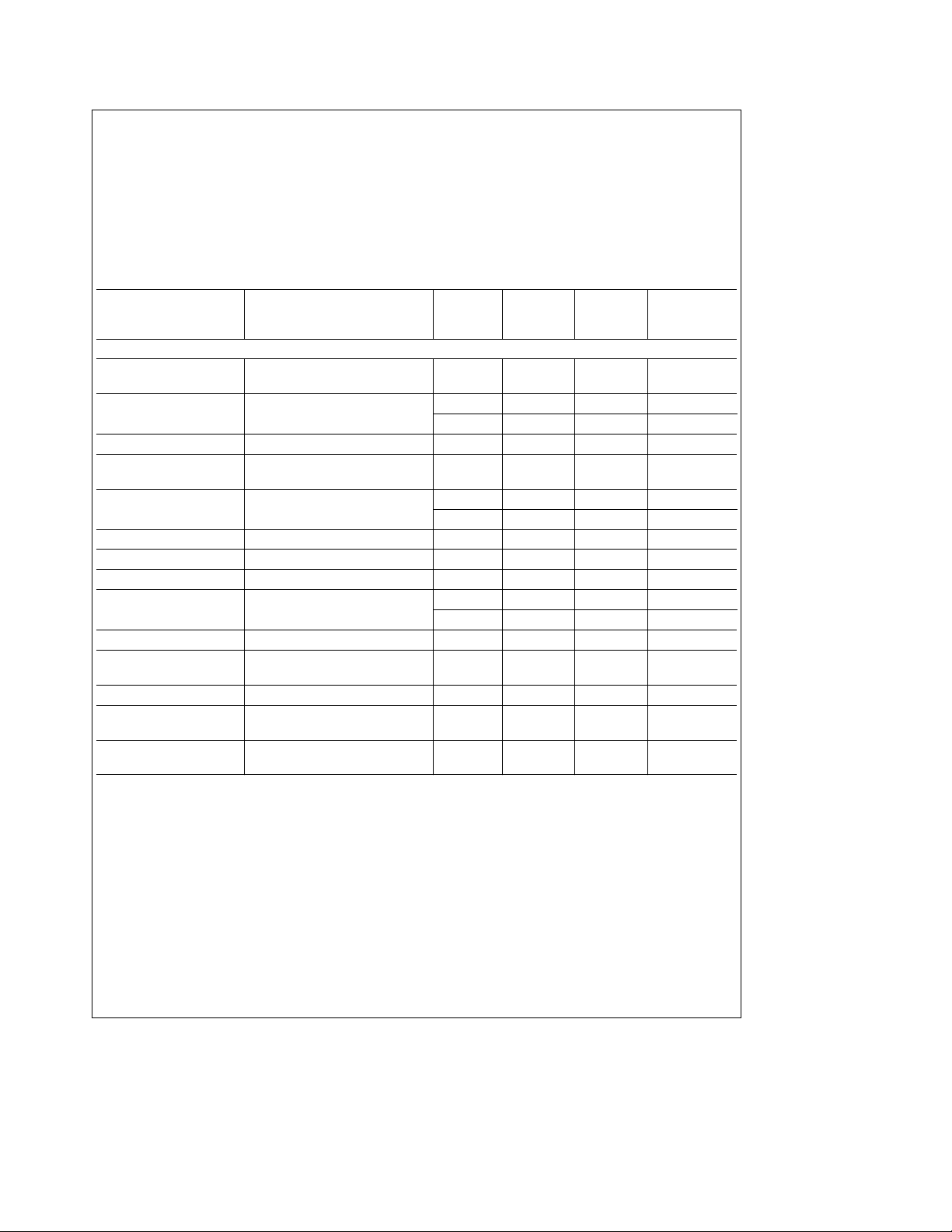
Electrical Characteristics
e
V
14V, I
IN
Parameter Conditions Typical Limit Limit Units
V
(Pin 11)
OUT
Output Voltage 5 mAsI
Line Regulation 9VsV
Load Regulation 5 mAsI
Output Impedance 250 mAdcand 10 mA
Quiescent Current I
Output Noise Voltage 10 Hz – 100 kHz, I
Long Term Stability 20 mV/1000 hr
Ripple Rejection f
Dropout Voltage I
Current Limit 0.92 0.75 A
Maximum Operational Continuous DC
Input Voltage
Maximum Line Transient V
Reverse Polarity V
Input Voltage DC
Reverse Polarity Input Ts100 ms, R
Voltage Transient
OUT
e
5 mA, C
OUT
e
10 mF, T
e
25§C (Note 6) unless otherwise indicated
j
Tested Design
(Note 2) (Note 3)
s
500 mA
o
6VsV
7VsV
f
I
I
s
26V 5.15 5.25 V
IN
s
16V 2 25 mV
IN
s
26V 5 50 mV
IN
s
500 mA 12 50 mV
OUT
,
e
120 Hz
o
e
500 mA 38 100 mA
OUT
e
250 mA 14 50 mA
OUT
e
120 Hz 70 60 dB
o
e
500 mA 0.53 0.80 1.00 V
OUT
e
250 mA 0.28 0.50 0.60 V
OUT
rms
e
100 mA 100 mV
OUT
5.00
24 mX
4.85 4.75 V
32 26 26 V
OUT
OUT
s
t
6V, R
b
OUT
0.6V, R
OUT
e
100X 45 35 35 V
e
100X
OUT
e
100X
b
30
b
55
b
15
b
35
b
15 V
b
35 V
min
max
max
max
max
max
max
min
max
max
min
min
min
min
min
2
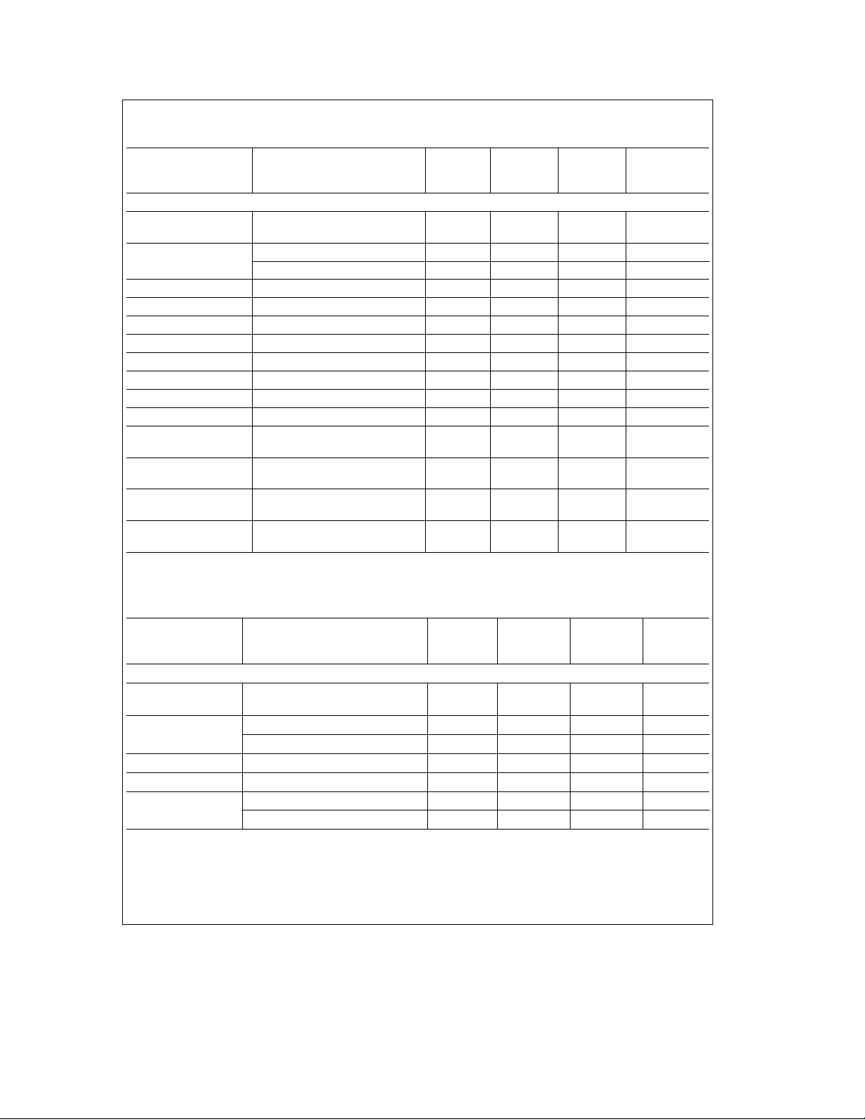
Electrical Characteristics (Continued)
e
V
IN
Parameter Conditions Typical Limit Limit Units
V
(Pin 10)
buffer
Output Voltage 5 mAsI
Line Regulation 9VsV
Load Regulation 5 mAsI
Output Impedance 50 mAdcand 10 mA
Quiescent Current I
Output Noise Voltage 10 Hz–100 kHz, I
Long Term Stability 20 mV/1000 hr
Ripple Rejection f
Dropout Voltage I
Current Limit 0.23 0.15 A
Maximum Operational Continuous DC
Input Voltage
Maximum Line V
Transient
Reverse Polarity V
Input Voltage DC
Reverse Polarity Input Ts100 ms, R
Voltage Transient
14V, I
buf
e
5 mA, C
buf
e
10 mF, T
e
25§C (Note 6) unless otherwise indicated
j
Tested Design
(Note 2) (Note 3)
s
100 mA
o
6VsV
7VsV
s
26V 5.15 5.25 V
IN
s
16V 2 25 mV
IN
s
26V 5 50 mV
IN
s
100 mA 15 50 mV
buf
, 200 mX
rms
e
100 mA 8.0 15.0 mA
buf
e
100 mA 100 mV
OUT
e
120 Hz 70 60 dB
o
e
100 mA 0.35 0.50 0.60 V
buf
5.00
4.85 4.75 V
32 26 26 V
buf
buf
s
t
6V, R
b
0.6V, R
buf
buf
e
buf
100X
e
e
100X
100X
45 35 35 V
b
30
b
55
b
15
b
35
b
b
15 V
35 V
min
max
max
max
max
max
min
max
min
min
min
min
min
Electrical Characteristics
e
V
14V, I
IN
Parameter Conditions Typical Limit Limit Units
V
(Pin 9)
standby
Output Voltage 1 mAsI
Line Regulation 9VsV
Load Regulation 0.5 mAsI
Output Impedance 5 mAdcand1mA
Quiescent Current I
stby
e
1 mA, C
stby
e
10 mF, T
e
25§C (Note 6) unless otherwise indicated
j
Tested Design
(Note 2) (Note 3)
s
7.5 mA
o
6VsV
7VsV
I
s
26V 5.15 5.25 V
IN
s
16V 2 25 mV
IN
s
26V 5 50 mV
IN
s
7.5 mA 6 50 mV
stby
e
120 Hz 0.9 X
rms,fo
e
7.5 mA 1.2 2.0 mA
stby
e
2 mA 0.9 1.5 mA
stby
5.00
4.85 4.75 V
3
min
max
max
max
max
max
max
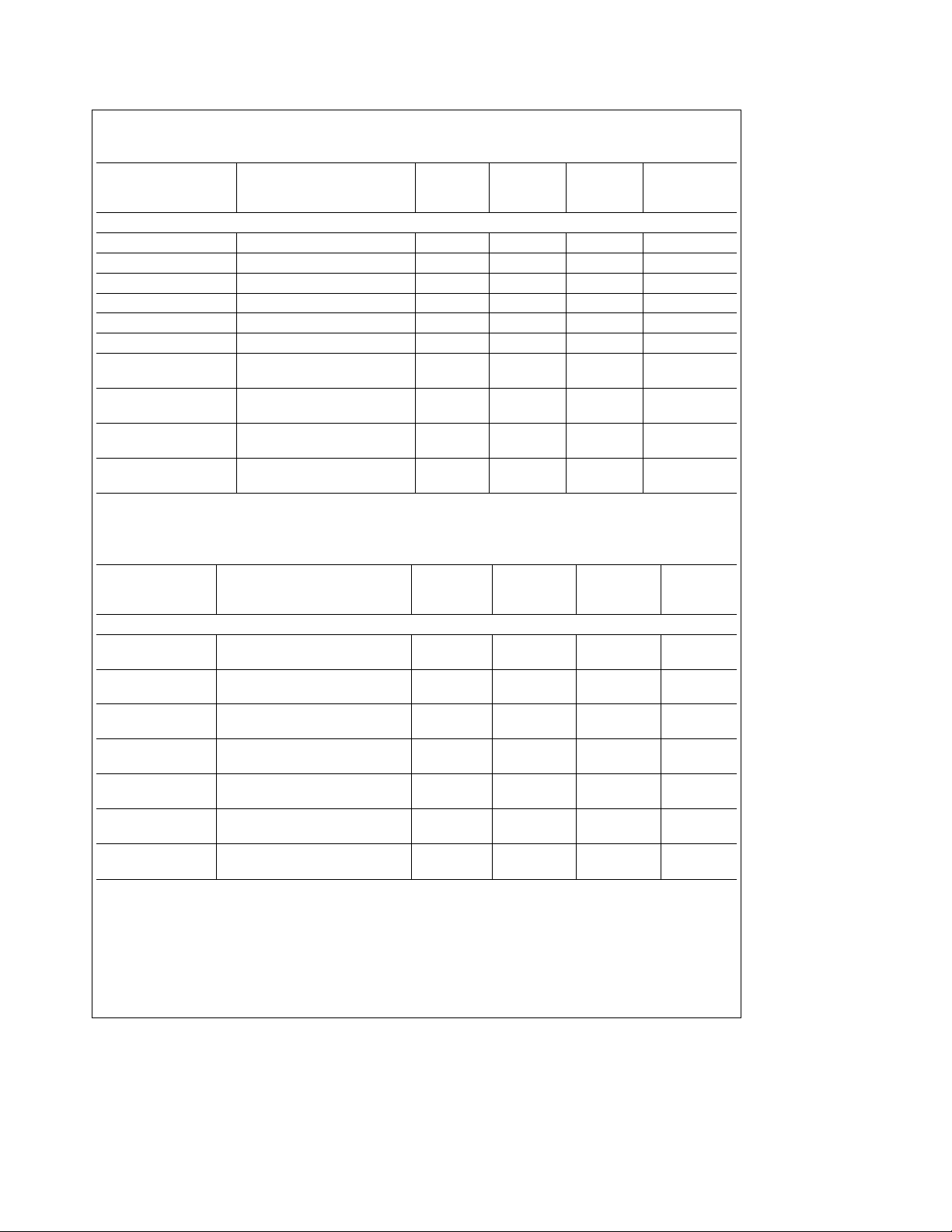
Electrical Characteristics (Continued)
e
14V, I
V
IN
Parameter Conditions Typical Limit Limit Units
V
(Continued)
standby
Output Noise Voltage 10 Hz –100 kHz, I
Long Term Stability 20 mV/1000 hr
Ripple Rejection f
Dropout Voltage I
Dropout Voltage I
Current Limit 15 12 mA
Maximum Operational 4.5VsV
Input Voltage R
Maximum Line V
Transient R
Reverse Polarity V
Input Voltage DC R
Reverse Polarity Input Ts100 ms, R
Voltage Transient
stby
e
1 mA, C
stby
e
10 mF, T
e
25§C (Note 6) unless otherwise indicated
j
Tested Design
(Note 2) (Note 3)
e
1 mA 100 mV
stby
e
120 Hz 70 60 dB
o
e
1 mA 0.26 0.50 0.50 V
stby
e
7.5 mA 0.38 0.60 0.70 V
stby
s
6V
stby
stby
stby
stby
stby
e
s
e
t
e
stby
1000X
6V,
1000X
b
0.6V,
1000X
stby
e
1000X
45 35 35 V
45 35 35 V
b
30
b
55
b
15
b
35
b
b
15 V
35 V
Electrical Characteristics
e
V
IN
Parameter Conditions Typical Limit Limit Units
Tracking and Isolation
Tracking I
V
OUT–Vstby
Tracking I
V
buf–Vstby
Tracking I
V
OUT–Vbuf
Isolation* R
V
buf
Isolation* R
V
stby
Isolation* R
V
OUT
Isolation* R
V
stby
*Isolation refers to the ability of the specified output to remain within the tested limits when the other output is shorted to ground.
14V, T
from V
from V
from V
from V
e
25§C (Note 6) C
j
OUT
OUT
buf
buf
OUT
I
stby
OUT
I
stby
OUT
I
stby
OUT
OUT
buf
buf
OUT
s
500 mA, I
s
7.5 mA
e
5 mA, I
s
7.5 mA
s
500 mA, I
e
1mA
e
e
e
1X,I
e
1X,I
e
1X,I
1X,I
10 mF, C
buf
buf
buf
s
buf
stby
s
OUT
s
stby
e
s
100 mA,
s
100 mA
s
7.5 mA
500 mA
7.5 mA
e
buf
5 mA,
100 mA,
10 mF, C
e
10 mF unless otherwise specified
stby
Tested Design
(Note 2) (Note 3)
g
g
g
5.00
5.00
5.00
5.00
30
30
30
g
g
g
4.50 V
5.50 V
4.50 V
5.50 V
4.50 V
5.50 V
4.50 V
5.50 V
100 mV
100 mV
100 mV
min
max
max
min
min
min
min
min
max
max
max
min
max
min
max
min
max
min
max
4
Electrical Characteristics (Continued)
e
14V, I
V
IN
otherwise specified
Parameter Conditions Typical Limit Limit Units
Computer Monitor/Reset Functions
I
Low V
reset
V
Low V
reset
R
t voltage
Power On Reset VmP
Delay (T
V
Low (Note 4) 4.00 3.60 V
OUT
Reset Threshold
V
High (Note 4) 5.50 5.25 V
OUT
Reset Threshold
Reset Output VmP
Leakage
mP
Input VmP
mon
Current (Pin 4)
mP
Input 1.22 0.80 0.80 V
mon
Threshold Voltage
mP Monitor Reset VmP
Oscillator Period (T
mP Monitor Reset VmP
Oscillator Pulse Width (RESET
Minimum mP Monitor (Note 5)
Input Pulse Width
Reset Fall Time R
Reset Rise Time R
On/Off Switch Input V
Current (Pin 8)
On/Off Switch Input 1.22 0.80 0.80 V
Threshold Voltage
Note 1: Thermal resistance without a heatsink for junction-to-case temperature is 3§C/W. Thermal resistance case-to-ambient is 40§C/W.
Note 2: Tested Limits are guaranteed and 100% production tested.
Note 3: Design Limits are guaranteed (but not 100% production tested) over the indicated temperature and supply voltage range. These limits are not used to
calculate outgoing quality levels.
Note 4: An internal comparator detects when the main regulator output (V
Reset Error Flag is held low until the error condition has terminated. The Reset Error Flag is then allowed to go high again after a delay set by R
Applications Section.)
Note 5: This parameter is a measure of how short a pulse can be detected at the mP Monitor Input. This parameter is primarily influenced by the value of C
(See Typical Performance Characteristics and Applications Section.)
Note 6: To ensure constant junction temperature, low duty cycle pulse testing is used.
OUT
e
5 mA, I
buf
e
5 mA, I
stby
e
5 mA, R
t
e
130k, C
e
t
0.33 mF, C
mon
e
0.47 mF, T
Tested Design
(Note 2) (Note 3)
e
IN
e
IN
4V, V
4V, I
e
0.4V 5 2 1 mA
rst
e
1 mA 0.10 0.40 V
rst
(Pin 2) 1.22 1.15 V
1.22 1.30 V
e
5V 50 45 ms
mon
e
1.2 RtCt)
dly
50 55 ms
4.00 4.40 V
5.50 6.00 V
VmP
mon
mon
mon
e
e
e
e
5V, V
12V
rst
0.01 1 mA
2.4V 7.5 25 mA
0.4V 0.01 10 mA
1.22 2.00 2.00 V
e
0V 50 45 ms
mon
e
window
0.82 RtC
e
0V 1.0 0.7 0.5 ms
mon
e
2000 C
pw
mon
mon
)
)
50 55 ms
1.0 1.3 2.0 ms
2 ms
e
rst
e
rst
e
ON
e
V
ON
e
10k, V
rst
e
10k, V
rst
2.4V 7.5 25 mA
0.4V 0.01 10 mA
5V, C
5V, C
s
10 pF 0.20 1.00 ms
rst
s
10 pF 0.60 1.00 ms
rst
1.22 2.00 2.00 V
) drops below 4.0V or rises above 5.5V. If either condition exists at the output, the
OUT
e
25§C (Note 6) unless
j
t
and Ct. (See
max
min
max
max
min
max
min
max
max
max
max
min
max
max
max
max
max
max
max
max
min
max
min
min
min
min
mon
.
5
 Loading...