NSC LM2936-3.0MDC, LM2936Z-3.0, LM2936MX-3.0, LM2936MPX-3.0, LM2936MP-3.0 Datasheet
...
LM2936-3.0
Ultra-Low Quiescent Current 3.0V Regulator
General Description
The LM2936-3.0 ultra-low quiescent current regulator features low dropout voltage and low current in the standby
mode. With less than 20 µA quiescent current at a 100 µA
load, the LM2936-3.0 is ideally suited for automotive and
other battery operated systems. The LM2936-3.0 retains all
of the features that are common to low dropout regulators
including a low dropout PNP pass device, short circuit protection, reverse battery protection, and thermal shutdown.
The LM2936-3.0 has a 40V maximum operating voltage
limit, a −40˚C to +125˚C operating temperature range, and
±
3% output voltage tolerance over the entire output current,
input voltage, and temperature range. The LM2936-3.0 is
available in a TO-92 package, a SO-8 surface mount package, as well as SOT-223 and TO-252 surface mount power
packages.
Features
n Ultra low quiescent current (IQ≤ 20 µA for IO= 100 µA)
n Fixed 3.0V, 50 mA output
n
±
2% Initial output tolerance
n
±
3% Output tolerance over line, load, and temperature
n Dropout voltage typically 200 mV
@
IO=50mA
n Reverse battery protection
n −50V reverse transient protection
n Internal short circuit current limit
n Internal thermal shutdown protection
n 40V operating voltage limit
n 60V operating voltage limit for LM2936HV
n Shutdown pin available with LM2936BM package
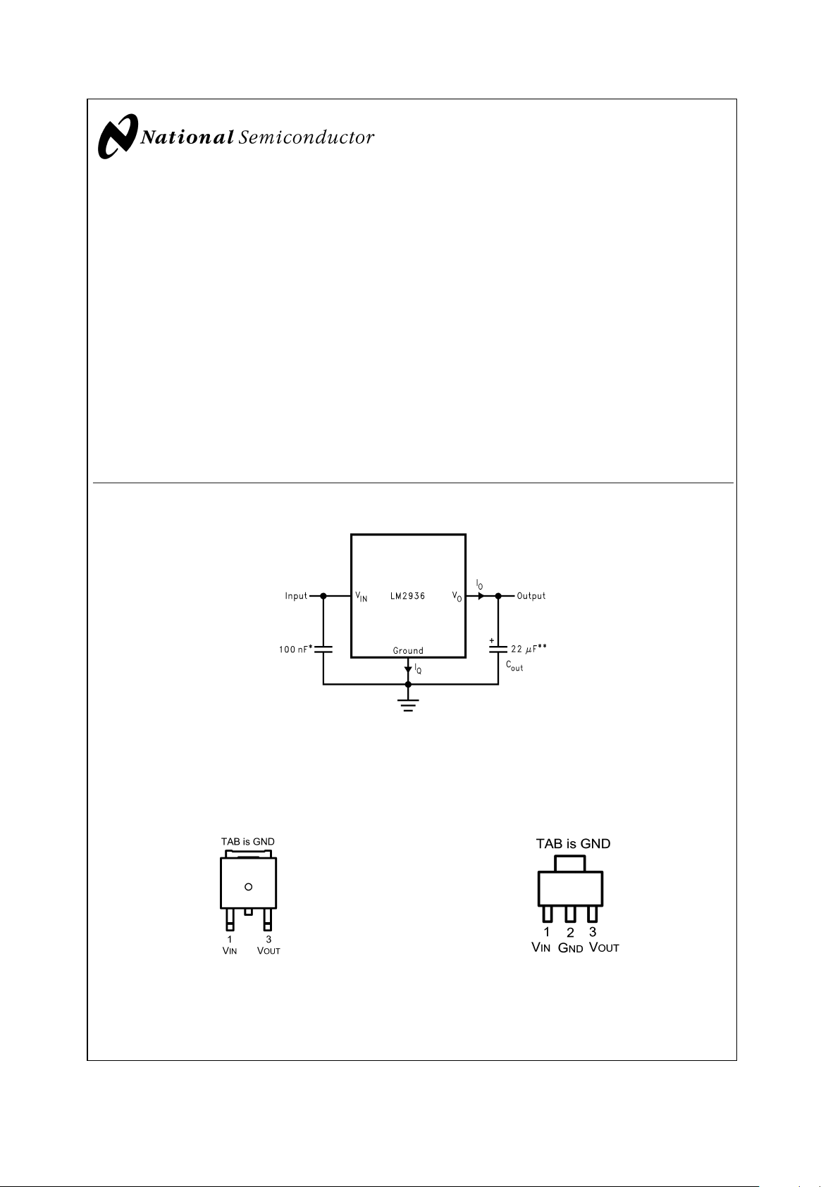
Typical Application
20001601
* Required if regulator is located more than 2" from power supply filter capacitor.
*
*
Required for stability. Must be rated for 22 µF minimum over intended operating temperature range. Effective series resistance (ESR) is critical, see
curve. Locate capacitor as close as possible to the regulator output and ground pins. Capacitance may be increased without bound.
Connection Diagrams
TO-252 SOT-223
20001625
Top View
Order Number LM2936DT-3.0
See NS Package Number TD03B
20001626
Top View
Order Number LM2936MP-3.0
See NS Package Number MA04A
June 2002
LM2936-3.0 Ultra-Low Quiescent Current 3.0V Regulator
© 2002 National Semiconductor Corporation DS200016 www.national.com

Connection Diagrams (Continued)
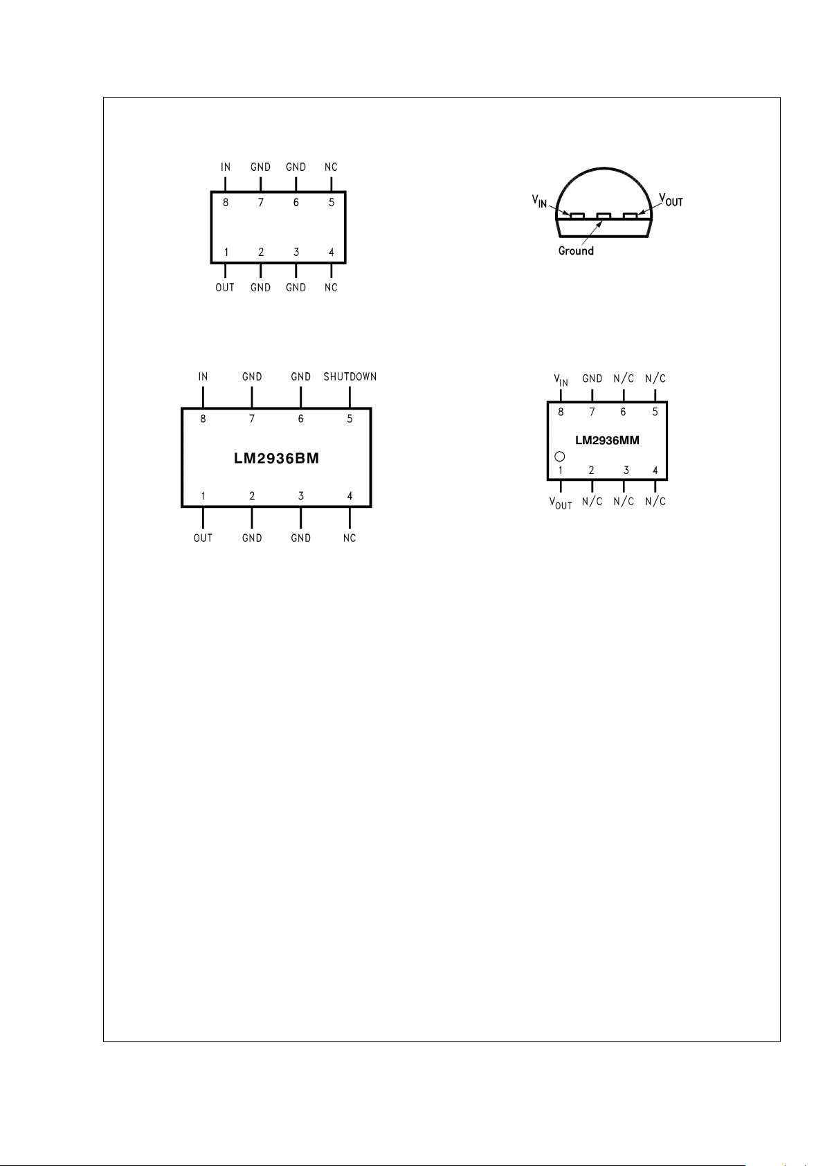
8-Pin SO (M) TO-92
20001606
Top View
Order Number LM2936M-3.0
See NS Package Number M08A
20001602
Bottom View
Order Number LM2936Z-3.0
See NS Package Number Z03A
8-Pin SO (M) 8-Pin SOIC (MM)
20001628
Top View
Order Number LM2936BM-3.0, LM2936HVBMA-3.0
See NS Package Number MO8A
20001629
Top View
Order Number LM2936MM-3.0
See NS Package Number MUA08A
LM2936-3.0
www.national.com 2

Absolute Maximum Ratings (Note 1)
If Military/Aerospace specified devices are required,
please contact the National Semiconductor Sales Office/
Distributors for availability and specifications.
Input Voltage (Survival) +60V, −50V
ESD Susceptibility (Note 2) 2000V
Power Dissipation (Note 3) Internally limited
Junction Temperature (T
Jmax
) 150˚C
Storage Temperature Range −65˚C to +150˚C
Lead Temperature (Soldering, 10
sec.) 260˚C
Operating Ratings
Operating Temperature Range −40˚C to +125˚C
Maximum Operating Input Voltage LM2936 +40V
Maximum Operating Input Voltage LM2936HV only +60V
Maximum Shutdown Pin Voltage LM2936BM only
0V to 40V
MSO-8 (MUA08A) θ
JA
200˚C/W
TO-92 (Z03A) θ
JA
195˚C/W
SO-8 (M08A) θ
JA
140˚C/W
SO-8 (M08A) θ
JC
45˚C/W
TO-252 (TD03B) θ
JA
126˚C/W
TO-252 (TD03B) θ
JC
6˚C/W
SOT-223 (MA04A) θ
JA
149˚C/W
SOT-223 (MA04A) θ
JC
36˚C/W
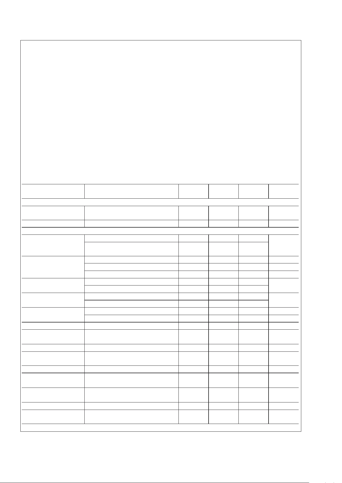
Electrical Characteristics
VIN= 14V, IO= 10 mA, TJ= 25˚C, unless otherwise specified. Boldface limits apply over entire operating temperature range
Parameter Conditions
Min
(Note 5)
Typical
(Note 4)
Max (Note
5)
Units
LM2936HV Only
Output Voltage 5.5V ≤ V
IN
≤ 48V,
100 µA ≤ I
O
≤ 50 mA (Note 6)
2.910 3.000 3.090 V
Line Regulation 6V ≤ V
IN
≤ 60V, IO= 1mA 10 30 mV
All LM2936
Output Voltage 2.940 3.000 3.060
V
4.0V ≤ V
IN
≤ 26V,
100µA ≤ I
O
≤ 50mA (Note 6)
2.910 3.000 3.090
Quiescent Current I
O
= 100 µA, 8V ≤ VIN≤ 24V 15 20 µA
I
O
= 10 mA, 8V ≤ VIN≤ 24V 0.20 0.50 mA
I
O
= 50 mA, 8V ≤ VIN≤ 24V 1.5 2.5 mA
Line Regulation 9V ≤ V
IN
≤ 16V 5 10 mV
6V ≤ V
IN
≤ 40V, IO= 1 mA 10 30
Load Regulation 100 µA ≤ I
O
≤ 5mA 10 30 mV
5mA≤ I
O
≤ 50 mA 10 30
Dropout Voltage I
O
= 100 µA 0.05 0.10 V
I
O
= 50 mA 0.20 0.40 V
Short Circuit Current V
O
= 0V 65 120 250 mA
Output Impedance I
O
= 30 mAdc and 10 mArms, 450 mΩ
f = 1000 Hz
Output Noise Voltage 10 Hz– 100 kHz 500 µV
Long Term Stability 20 mV/1000
Hr
Ripple Rejection V
ripple
=1V
rms,fripple
= 120 Hz −40 −60 dB
Reverse Polarity R
L
= 500Ω, T = 1 ms −50 −80 V
Transient Input Voltage
Output Voltage with V
IN
= −15V, RL= 500Ω 0.00 −0.30 V
Reverse Polarity Input
Maximum Line Transient R
L
= 500Ω,VO≤ 3.30V 60 V
Output Bypass
Capacitance (C
OUT
) ESR
C
OUT
= 22µF
0.1mA ≤ I
OUT
≤ 50mA
0.3 8 Ω
LM2936-3.0
www.national.com3
 Loading...