

LM2936-3.0
Ultra-Low Quiescent Current 3.0V Regulator
General Description
The LM2936-3.0 ultra-low quiescent current regulator features low dropout voltage and low current in the standby
mode. With less than 20 µA quiescent current at a 100 µA
load, the LM2936-3.0 is ideally suited for automotive and
other battery operated systems. The LM2936-3.0 retains all
of the features that are common to low dropout regulators
including a low dropout PNP pass device, short circuit protection, reverse battery protection, and thermal shutdown.
The LM2936-3.0 has a 40V maximum operating voltage
limit, a −40˚C to +125˚C operating temperature range, and
±
3% output voltage tolerance over the entire output current,
input voltage, and temperature range. The LM2936-3.0 is
available in a TO-92 package, a SO-8 surface mount package, as well as SOT-223 and TO-252 surface mount power
packages.
Features
n Ultra low quiescent current (IQ≤ 20 µA for IO= 100 µA)
n Fixed 3.0V, 50 mA output
n
±
2% Initial output tolerance
n
±
3% Output tolerance over line, load, and temperature
n Dropout voltage typically 200 mV
@
IO=50mA
n Reverse battery protection
n −50V reverse transient protection
n Internal short circuit current limit
n Internal thermal shutdown protection
n 40V operating voltage limit
n 60V operating voltage limit for LM2936HV
n Shutdown pin available with LM2936BM package
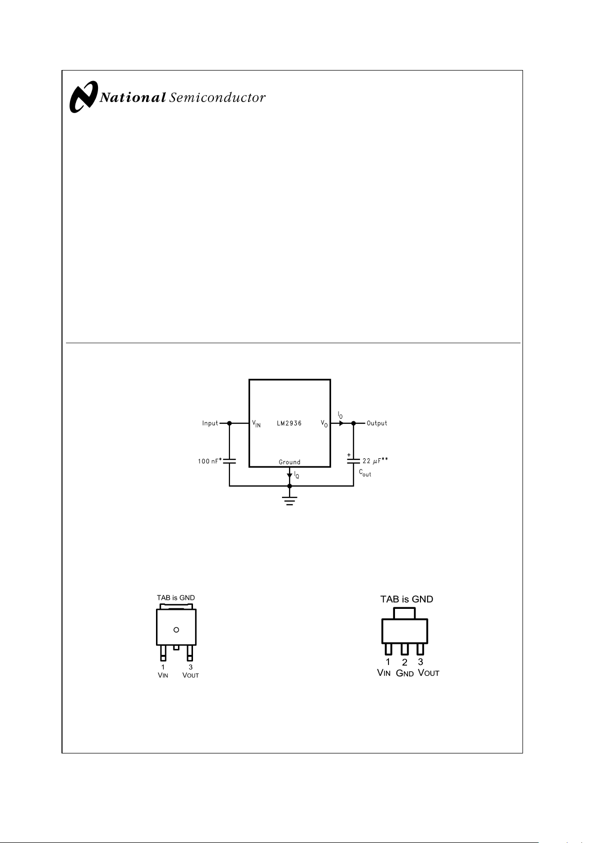
Typical Application
20001601
* Required if regulator is located more than 2" from power supply filter capacitor.
*
*
Required for stability. Must be rated for 22 µF minimum over intended operating temperature range. Effective series resistance (ESR) is critical, see
curve. Locate capacitor as close as possible to the regulator output and ground pins. Capacitance may be increased without bound.
Connection Diagrams
TO-252 SOT-223
20001625
Top View
Order Number LM2936DT-3.0
See NS Package Number TD03B
20001626
Top View
Order Number LM2936MP-3.0
See NS Package Number MA04A
June 2002
LM2936-3.0 Ultra-Low Quiescent Current 3.0V Regulator
© 2002 National Semiconductor Corporation DS200016 www.national.com
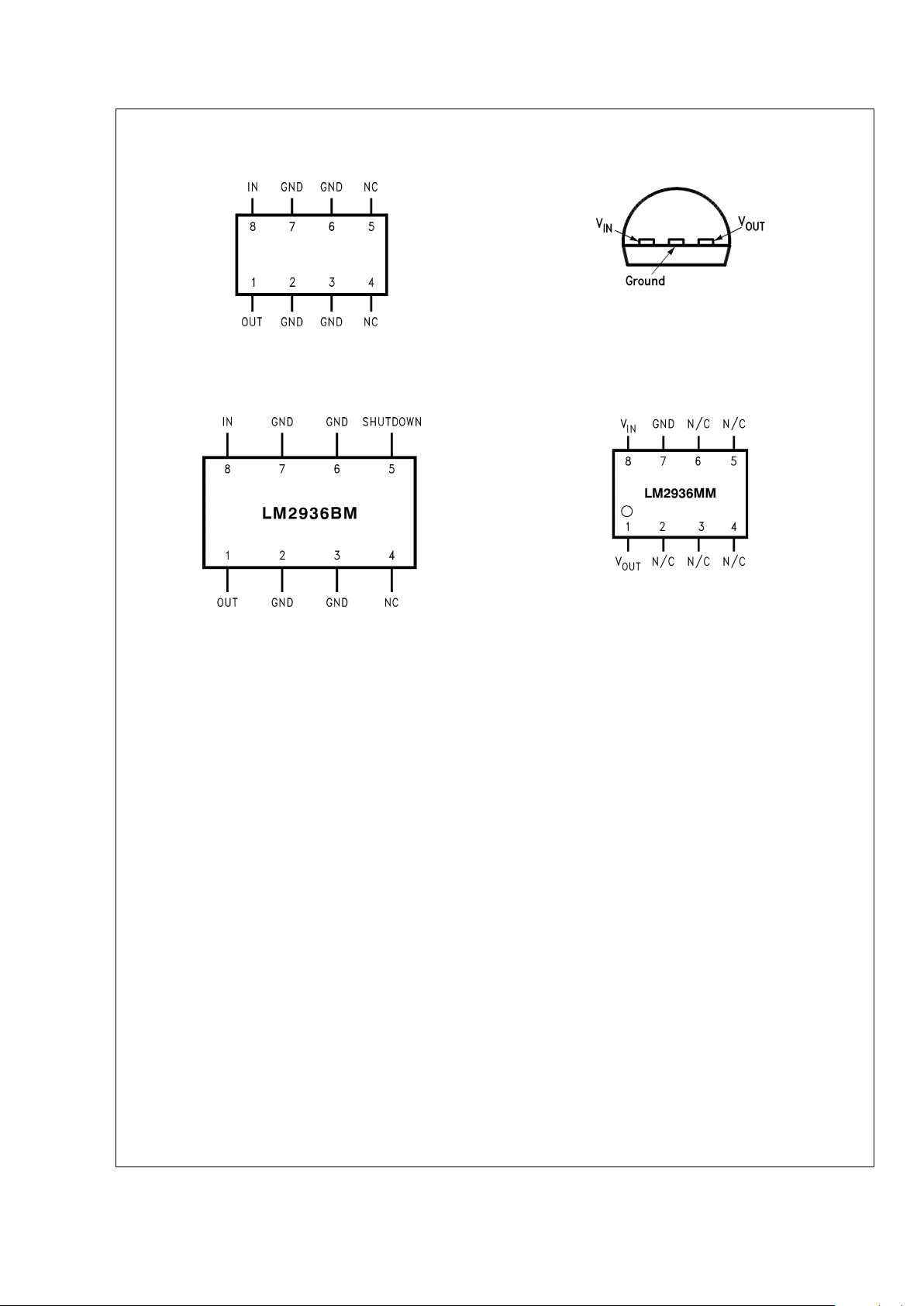
Connection Diagrams (Continued)
8-Pin SO (M) TO-92
20001606
Top View
Order Number LM2936M-3.0
See NS Package Number M08A
20001602
Bottom View
Order Number LM2936Z-3.0
See NS Package Number Z03A
8-Pin SO (M) 8-Pin SOIC (MM)
20001628
Top View
Order Number LM2936BM-3.0, LM2936HVBMA-3.0
See NS Package Number MO8A
20001629
Top View
Order Number LM2936MM-3.0
See NS Package Number MUA08A
LM2936-3.0
www.national.com 2
Absolute Maximum Ratings (Note 1)
If Military/Aerospace specified devices are required,
please contact the National Semiconductor Sales Office/
Distributors for availability and specifications.
Input Voltage (Survival) +60V, −50V
ESD Susceptibility (Note 2) 2000V
Power Dissipation (Note 3) Internally limited
Junction Temperature (T
Jmax
) 150˚C
Storage Temperature Range −65˚C to +150˚C
Lead Temperature (Soldering, 10
sec.) 260˚C
Operating Ratings
Operating Temperature Range −40˚C to +125˚C
Maximum Operating Input Voltage LM2936 +40V
Maximum Operating Input Voltage LM2936HV only +60V
Maximum Shutdown Pin Voltage LM2936BM only
0V to 40V
MSO-8 (MUA08A) θ
JA
200˚C/W
TO-92 (Z03A) θ
JA
195˚C/W
SO-8 (M08A) θ
JA
140˚C/W
SO-8 (M08A) θ
JC
45˚C/W
TO-252 (TD03B) θ
JA
126˚C/W
TO-252 (TD03B) θ
JC
6˚C/W
SOT-223 (MA04A) θ
JA
149˚C/W
SOT-223 (MA04A) θ
JC
36˚C/W
Electrical Characteristics
VIN= 14V, IO= 10 mA, TJ= 25˚C, unless otherwise specified. Boldface limits apply over entire operating temperature range
Parameter Conditions
Min
(Note 5)
Typical
(Note 4)
Max (Note
5)
Units
LM2936HV Only
Output Voltage 5.5V ≤ V
IN
≤ 48V,
100 µA ≤ I
O
≤ 50 mA (Note 6)
2.910 3.000 3.090 V
Line Regulation 6V ≤ V
IN
≤ 60V, IO= 1mA 10 30 mV
All LM2936
Output Voltage 2.940 3.000 3.060
V
4.0V ≤ V
IN
≤ 26V,
100µA ≤ I
O
≤ 50mA (Note 6)
2.910 3.000 3.090
Quiescent Current I
O
= 100 µA, 8V ≤ VIN≤ 24V 15 20 µA
I
O
= 10 mA, 8V ≤ VIN≤ 24V 0.20 0.50 mA
I
O
= 50 mA, 8V ≤ VIN≤ 24V 1.5 2.5 mA
Line Regulation 9V ≤ V
IN
≤ 16V 5 10 mV
6V ≤ V
IN
≤ 40V, IO= 1 mA 10 30
Load Regulation 100 µA ≤ I
O
≤ 5mA 10 30 mV
5mA≤ I
O
≤ 50 mA 10 30
Dropout Voltage I
O
= 100 µA 0.05 0.10 V
I
O
= 50 mA 0.20 0.40 V
Short Circuit Current V
O
= 0V 65 120 250 mA
Output Impedance I
O
= 30 mAdc and 10 mArms, 450 mΩ
f = 1000 Hz
Output Noise Voltage 10 Hz– 100 kHz 500 µV
Long Term Stability 20 mV/1000
Hr
Ripple Rejection V
ripple
=1V
rms,fripple
= 120 Hz −40 −60 dB
Reverse Polarity R
L
= 500Ω, T = 1 ms −50 −80 V
Transient Input Voltage
Output Voltage with V
IN
= −15V, RL= 500Ω 0.00 −0.30 V
Reverse Polarity Input
Maximum Line Transient R
L
= 500Ω,VO≤ 3.30V 60 V
Output Bypass
Capacitance (C
OUT
) ESR
C
OUT
= 22µF
0.1mA ≤ I
OUT
≤ 50mA
0.3 8 Ω
LM2936-3.0
www.national.com3

Electrical Characteristics (Continued)
VIN= 14V, IO= 10 mA, TJ= 25˚C, unless otherwise specified. Boldface limits apply over entire operating temperature range
Parameter Conditions
Min
(Note 5)
Typical
(Note 4)
Max (Note
5)
Units
Shutdown Input - LM2936BM Only
Output Voltage, V
OUT
Output Off, VSD= 2.4V 0 0.010 V
Shutdown High Threshold
Voltage, V
IH
Output Off, R
LOAD
= 500Ω 2.00 1.1 V
Shutdown Low Threshold
Voltage, V
IL
Output On, R
LOAD
= 500Ω 1.1 0.60 V
Shutdown High Current,
I
IH
Output Off, VSD= 2.4V, R
LOAD
= 500Ω 12 µA
Quiescent Current Output Off, V
SD
= 2.4V, R
LOAD
= 500Ω
Includes I
IH
Current
30 µA
Note 1: Absolute Maximum Ratings indicate limits beyond which damage to the device may occur. DC and AC electrical specifications do not apply when operating
the device beyond its specified operating ratings.
Note 2: Human body model, 100pF discharge through a 1.5kΩ resistor.
Note 3: The maximum power dissipation is a function of T
Jmax
, θJA, and TA. The maximum allowable power dissipation at any ambient temperature is
P
D
=(T
Jmax−TA
)/θJA. If this dissipation is exceeded, the die temperature will rise above 150˚C and the LM2936 will go into thermal shutdown.
Note 4: Typicals are at 25˚C (unless otherwise specified) and represent the most likely parametric norm.
Note 5: Datasheet min/max specification limits are guaranteed by design, test, or statistical analysis.
Note 6: To ensure constant junction temperature, pulse testing is used.
Typical Performance Characteristics
Maximum Power
Dissipation (TO-92) Dropout Voltage
20001607 20001608
Dropout Voltage Quiescent Current
20001609 20001610
LM2936-3.0
www.national.com 4

Typical Performance Characteristics (Continued)
Quiescent Current Quiescent Current
20001611
20001612
Quiescent Current Quiescent Current
20001613
20001614
Output Capacitor ESR Peak Output Current
20001615
20001616
LM2936-3.0
www.national.com5

Typical Performance Characteristics (Continued)
Peak Output Current Line Transient Response
20001617
20001619
Ripple Rejection Load Transient Response
20001621
20001622
Output Impedance
20001624
Applications Information
Unlike other PNP low dropout regulators, the LM2936 remains fully operational to 40V. Owing to power dissipation
characteristics of the available packages, full output current
cannot be guaranteed for all combinations of ambient temperature and input voltage.
The junction to ambient thermal resistance θ
JA
rating has
two distinct components: the junction to case thermal resistance rating θ
JC
; and the case to ambient thermal resistance
rating θ
CA
. The relationship is defined as: θJA= θJC+ θCA.
For the SO-8 and TO-252 surface mount packages the θ
JA
rating can be improved by using the copper mounting pads
on the printed circuit board as a thermal conductive path to
extract heat from the package.
LM2936-3.0
www.national.com 6

Applications Information (Continued)
On the SO-8 package the four ground pins are thermally
connected to the backside of the die. Adding approximately
0.04 square inches of 2 oz. copper pad area to these four
pins will improve the θ
JA
rating to approximately 110˚C/W. If
this extra pad are is placed directly beneath the package
there should not be any impact on board density.
On the TO-252 package the ground tab is thermally connected to the backside of the die. Adding 1 square inch of 2
oz. copper pad area directly under the ground tab will improve the θ
JA
rating to approximately 50˚C/W.
While the LM2936 has an internally set thermal shutdown
point of typically 150˚C, this is intended as a safety feature
only. Continuous operation near the thermal shutdown temperature should be avoided as it may have a negative affect
on the life of the device.
While the LM2936-3.0 will survive input transients to +60V,
output regulation is not guaranteed for input voltages greater
than 40V. The LM2936 will not withstand a output short
circuit with the input above 40V because of safe operating
area limitations in the internal PNP pass device. With input
voltages above 60V the LM2936 will break down with catastrophic effects on the regulator and possibly the load as
well. Do not use this device in a design where the input
operating voltage may exceed 40V, or where transients are
likely to exceed 60V.
Shutdown Pin
The LM2936BM has a pin for shutting down the regulator
output. Applying a Logic Level High (
>
2.0V) to the Shutdown
pin will cause the output to turn off. Leaving the Shutdown
pin open, connecting it to Ground, or applying a Logic Level
Low (
<
0.6V) will allow the regulator output to turn on.
LM2936-3.0
www.national.com7

Physical Dimensions inches (millimeters) unless otherwise noted
8-Lead Small Outline Molded Package (M)
NS Package Number M08A
TO-252 Package (DT)
NS Package Number TD03B
LM2936-3.0
www.national.com 8
Physical Dimensions inches (millimeters) unless otherwise noted (Continued)
SOT-223 Package (MP)
NS Package Number MA04A
3-Lead TO-92 Plastic Package (Z)
NS Package Number Z03A
LM2936-3.0
www.national.com9

Physical Dimensions inches (millimeters) unless otherwise noted (Continued)
8-Lead Mini SOIC package (MM)
NS Package Number MUA08A
LIFE SUPPORT POLICY
NATIONAL’S PRODUCTS ARE NOT AUTHORIZED FOR USE AS CRITICAL COMPONENTS IN LIFE SUPPORT
DEVICES OR SYSTEMS WITHOUT THE EXPRESS WRITTEN APPROVAL OF THE PRESIDENT AND GENERAL
COUNSEL OF NATIONAL SEMICONDUCTOR CORPORATION. As used herein:
1. Life support devices or systems are devices or
systems which, (a) are intended for surgical implant
into the body, or (b) support or sustain life, and
whose failure to perform when properly used in
accordance with instructions for use provided in the
labeling, can be reasonably expected to result in a
significant injury to the user.
2. A critical component is any component of a life
support device or system whose failure to perform
can be reasonably expected to cause the failure of
the life support device or system, or to affect its
safety or effectiveness.
National Semiconductor
Corporation
Americas
Email: support@nsc.com
National Semiconductor
Europe
Fax: +49 (0) 180-530 85 86
Email: europe.support@nsc.com
Deutsch Tel: +49 (0) 69 9508 6208
English Tel: +44 (0) 870 24 0 2171
Français Tel: +33 (0) 1 41 91 8790
National Semiconductor
Asia Pacific Customer
Response Group
Tel: 65-2544466
Fax: 65-2504466
Email: ap.support@nsc.com
National Semiconductor
Japan Ltd.
Tel: 81-3-5639-7560
Fax: 81-3-5639-7507
www.national.com
LM2936-3.0 Ultra-Low Quiescent Current 3.0V Regulator
National does not assume any responsibility for use of any circuitry described, no circuit patent licenses are implied and National reserves the right at any time without notice to change said circuitry and specifications.
 Loading...