NSC LM2907N-8, LM2907MX-8, LM2907M-8, LM2907N Datasheet
TL/H/7942
LM2907/LM2917 Frequency to Voltage Converter
February 1995
LM2907/LM2917 Frequency to Voltage Converter
General Description
The LM2907, LM2917 series are monolithic frequency to
voltage converters with a high gain op amp/comparator designed to operate a relay, lamp, or other load when the input
frequency reaches or exceeds a selected rate. The tachometer uses a charge pump technique and offers frequency
doubling for low ripple, full input protection in two versions
(LM2907-8, LM2917-8) and its output swings to ground for a
zero frequency input.
Advantages
Y
Output swings to ground for zero frequency input
Y
Easy to use; V
OUT
e
f
IN
c
V
CC
c
R1cC1
Y
Only one RC network provides frequency doubling
Y
Zener regulator on chip allows accurate and stable frequency to voltage or current conversion (LM2917)
Features
Y
Ground referenced tachometer input interfaces directly
with variable reluctance magnetic pickups
Y
Op amp/comparator has floating transistor output
Y
50 mA sink or source to operate relays, solenoids, meters, or LEDs
Y
Frequency doubling for low ripple
Y
Tachometer has built-in hysteresis with either differential input or ground referenced input
Y
Built-in zener on LM2917
Y
g
0.3% linearity typical
Y
Ground referenced tachometer is fully protected from
damage due to swings above V
CC
and below ground
Applications
Y
Over/under speed sensing
Y
Frequency to voltage conversion (tachometer)
Y
Speedometers
Y
Breaker point dwell meters
Y
Hand-held tachometer
Y
Speed governors
Y
Cruise control
Y
Automotive door lock control
Y
Clutch control
Y
Horn control
Y
Touch or sound switches
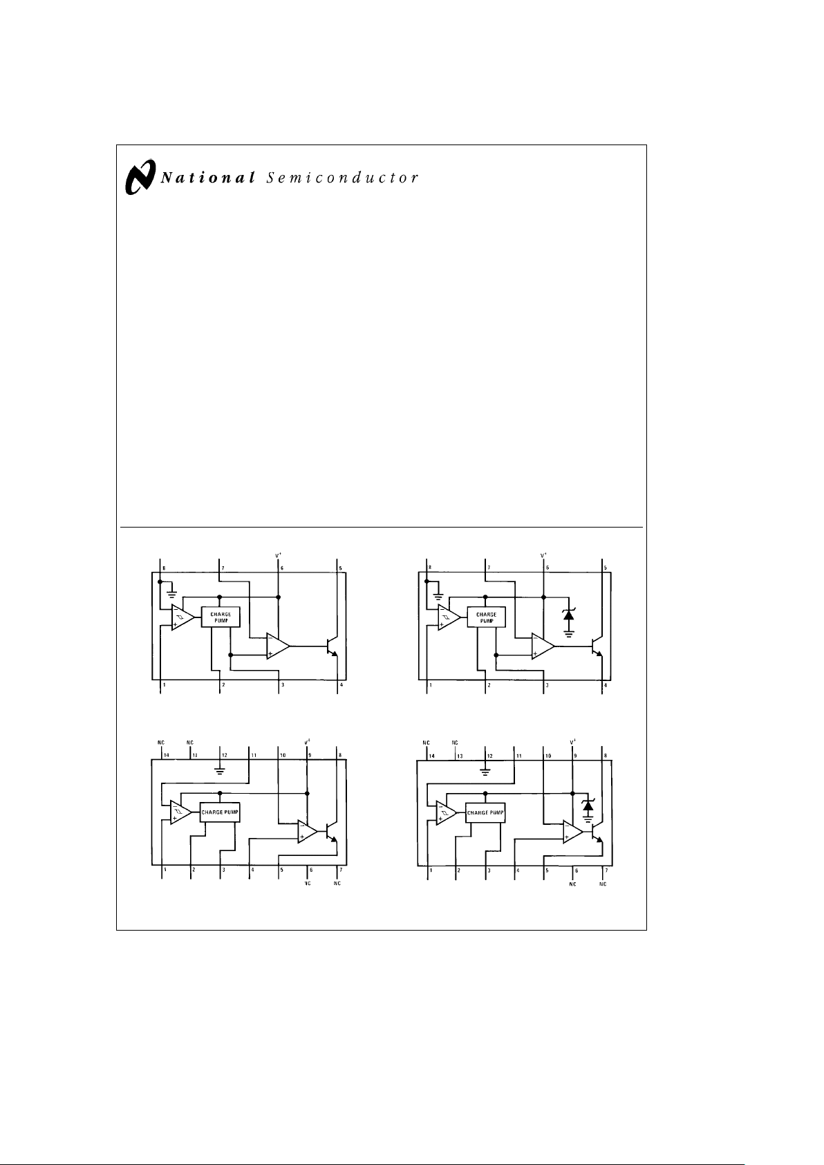
Block and Connection Diagrams Dual-In-Line and Small Outline Packages, Top Views
TL/H/7942– 1
Order Number LM2907M-8 or LM2907N-8
See NS Package Number M08A or N08E
TL/H/7942– 2
Order Number LM2917M-8 or LM2917N-8
See NS Package Number M08A or N08E
TL/H/7942– 3
Order Number LM2907N
See NS Package Number N14A
TL/H/7942– 4
Order Number LM2917M or LM2917N
See NS Package Number M14A or N14A
C
1995 National Semiconductor Corporation RRD-B30M115/Printed in U. S. A.
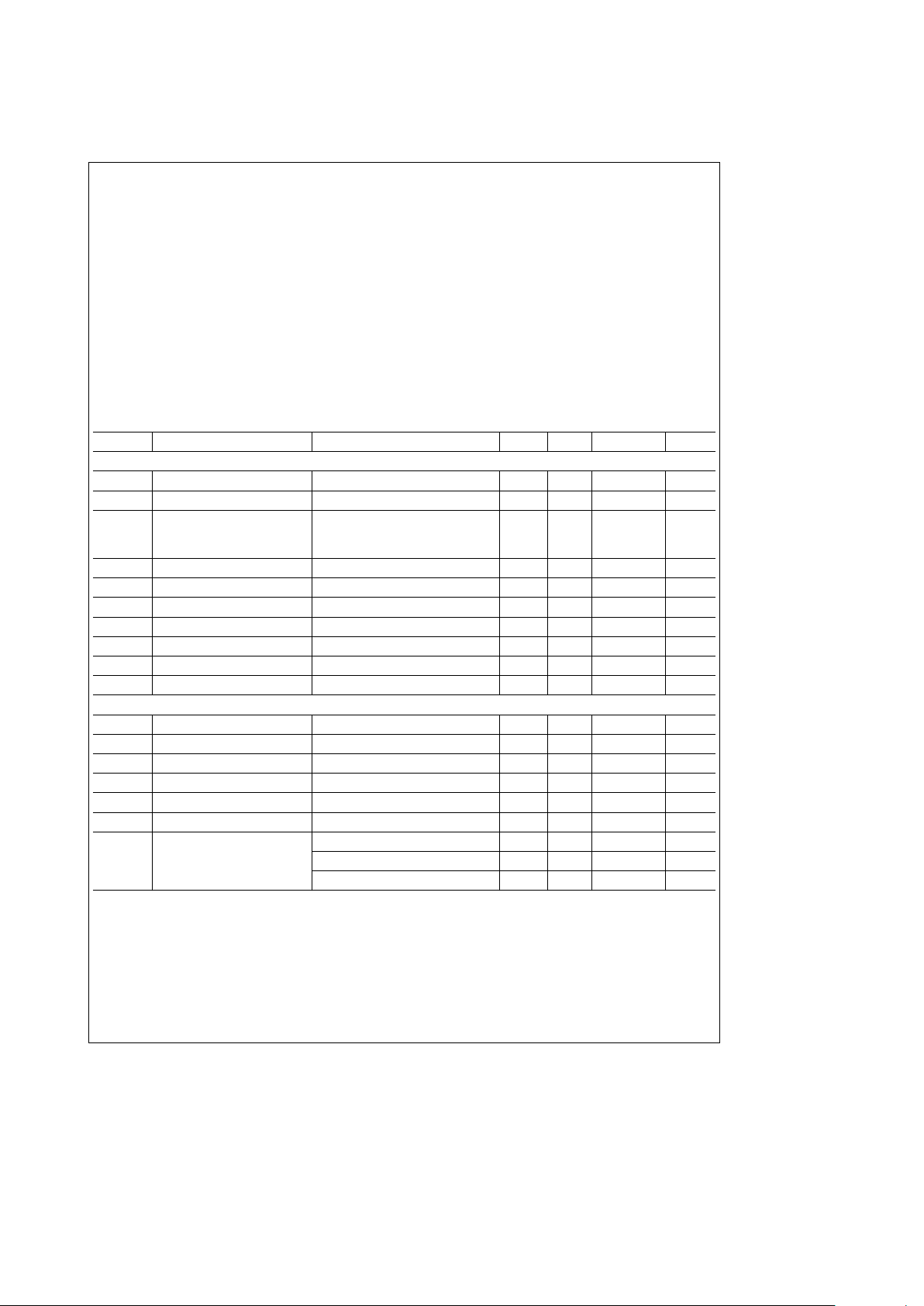
Absolute Maximum Ratings (Note 1)
If Military/Aerospace specified devices are required,
please contact the National Semiconductor Sales
Office/Distributors for availability and specifications.
Supply Voltage 28V
Supply Current (Zener Options) 25 mA
Collector Voltage 28V
Differential Input Voltage
Tachometer 28V
Op Amp/Comparator 28V
Input Voltage Range
Tachometer LM2907-8, LM2917-8
g
28V
LM2907, LM2917 0.0V to
a
28V
Op Amp/Comparator 0.0V to
a
28V
Power Dissipation
LM2907-8, LM2917-8 1200 mW
LM2907-14, LM2917-14 1580 mW
(See Note 1)
Operating Temperature Range
b
40§Ctoa85§C
Storage Temperature Range
b
65§Ctoa150§C
Soldering Information
Dual-In-Line Package
Soldering (10 seconds) 260
§
C
Small Outline Package
Vapor Phase (60 seconds) 215
§
C
Infrared (15 seconds) 220
§
C
See AN-450 ‘‘Surface Mounting Methods and Their Effect
on Product Reliability’’ for other methods of soldering surface mount devices.
Electrical Characteristics V
CC
e
12 VDC,T
A
e
25§C, see test circuit
Symbol Parameter Conditions Min Typ Max Units
TACHOMETER
Input Thresholds V
IN
e
250 mVp-p@1 kHz (Note 2)
g
10
g
25
g
40 mV
Hysteresis V
IN
e
250 mVp-p@1 kHz (Note 2) 30 mV
Offset Voltage V
IN
e
250 mVp-p@1 kHz (Note 2)
LM2907/LM2917 3.5 10 mV
LM2907-8/LM2917-8 5 15 mV
Input Bias Current V
IN
e
g
50 mV
DC
0.1 1 mA
V
OH
Pin 2 V
IN
ea
125 mVDC(Note 3) 8.3 V
V
OL
Pin 2 V
IN
eb
125 mVDC(Note 3) 2.3 V
I2,I
3
Output Current V2eV3e6.0V (Note 4) 140 180 240 mA
I
3
Leakage Current I2e0, V3e0 0.1 mA
K Gain Constant (Note 3) 0.9 1.0 1.1
Linearity f
IN
e
1 kHz, 5 kHz, 10 kHz (Note 5)
b
1.0 0.3
a
1.0 %
OP/AMP COMPARATOR
V
OS
V
IN
e
6.0V 3 10 mV
I
BIAS
V
IN
e
6.0V 50 500 nA
Input Common-Mode Voltage 0 V
CC
b
1.5V V
Voltage Gain 200 V/mV
Output Sink Current V
C
e
1.0 40 50 mA
Output Source Current V
E
e
V
CC
b
2.0 10 mA
Saturation Voltage I
SINK
e
5 mA 0.1 0.5 V
I
SINK
e
20 mA 1.0 V
I
SINK
e
50 mA 1.0 1.5 V
2
Electrical Characteristics V
CC
e
12 VDC,T
A
e
25§C, see test circuit (Continued)
Symbol Parameter Conditions Min Typ Max Units
ZENER REGULATOR
Regulator Voltage R
DROP
e
470X 7.56 V
Series Resistance 10.5 15 X
Temperature Stability
a
1 mV/§C
TOTAL SUPPLY CURRENT 3.8 6 mA
Note 1: For operation in ambient temperatures above 25§C, the device must be derated based on a 150§C maximum junction temperature and a thermal resistance
of 101
§
C/W junction to ambient for LM2907-8 and LM2917-8, and 79§C/W junction to ambient for LM2907-14 and LM2917-14.
Note 2: Hysteresis is the sum
a
V
TH
b(b
VTH), offset voltage is their difference. See test circuit.
Note 3: V
OH
is equal to */4cV
CC
b
1VBE,VOLis equal to (/4cV
CC
b
1VBEtherefore V
OH
b
V
OL
e
VCC/2. The difference, V
OH
b
VOL, and the mirror gain,
I
2/I3
, are the two factors that cause the tachometer gain constant to vary from 1.0.
Note 4: Be sure when choosing the time constant R1
c
C1 that R1 is such that the maximum anticipated output voltage at pin 3 can be reached with I
3
c
R1. The
maximum value for R1 is limited by the output resistance of pin 3 which is greater than 10 M X typically.
Note 5: Nonlinearity is defined as the deviation of V
OUT
(@pin 3) for f
IN
e
5 kHz from a straight line defined by the V
OUT
@
1 kHz and V
OUT
@
10 kHz.
C1
e
1000 pF, R1e68k and C2e0.22 mFd.
General Description (Continued)
The op amp/comparator is fully compatible with the tachometer and has a floating transistor as its output. This
feature allows either a ground or supply referred load of up
to 50 mA. The collector may be taken above V
CC
up to a
maximum V
CE
of 28V.
The two basic configurations offered include an 8-pin device
with a
ground referenced tachometer
input and an internal
connection between the tachometer output and the op amp
non-inverting input. This version is well suited for single
speed or frequency switching or fully buffered frequency to
voltage conversion applications.
The more versatile configurations provide differential tachometer input and uncommitted op amp inputs. With this
version the tachometer input may be floated and the op
amp becomes suitable for active filter conditioning of the
tachometer output.
Both of these configurations are available with an active
shunt regulator connected across the power leads. The regulator clamps the supply such that stable frequency to voltage and frequency to current operations are possible with
any supply voltage and a suitable resistor.
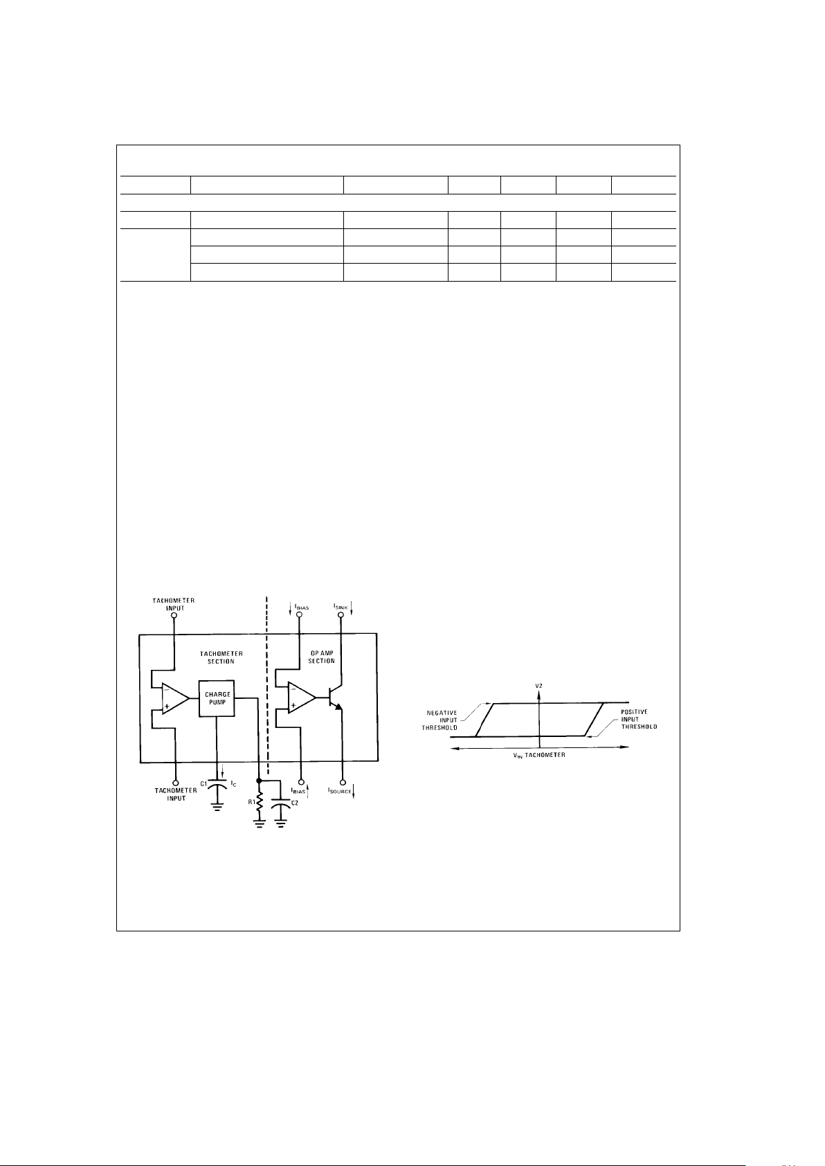
Test Circuit and Waveform
TL/H/7942– 6
Tachometer Input Threshold Measurement
TL/H/7942– 7
3
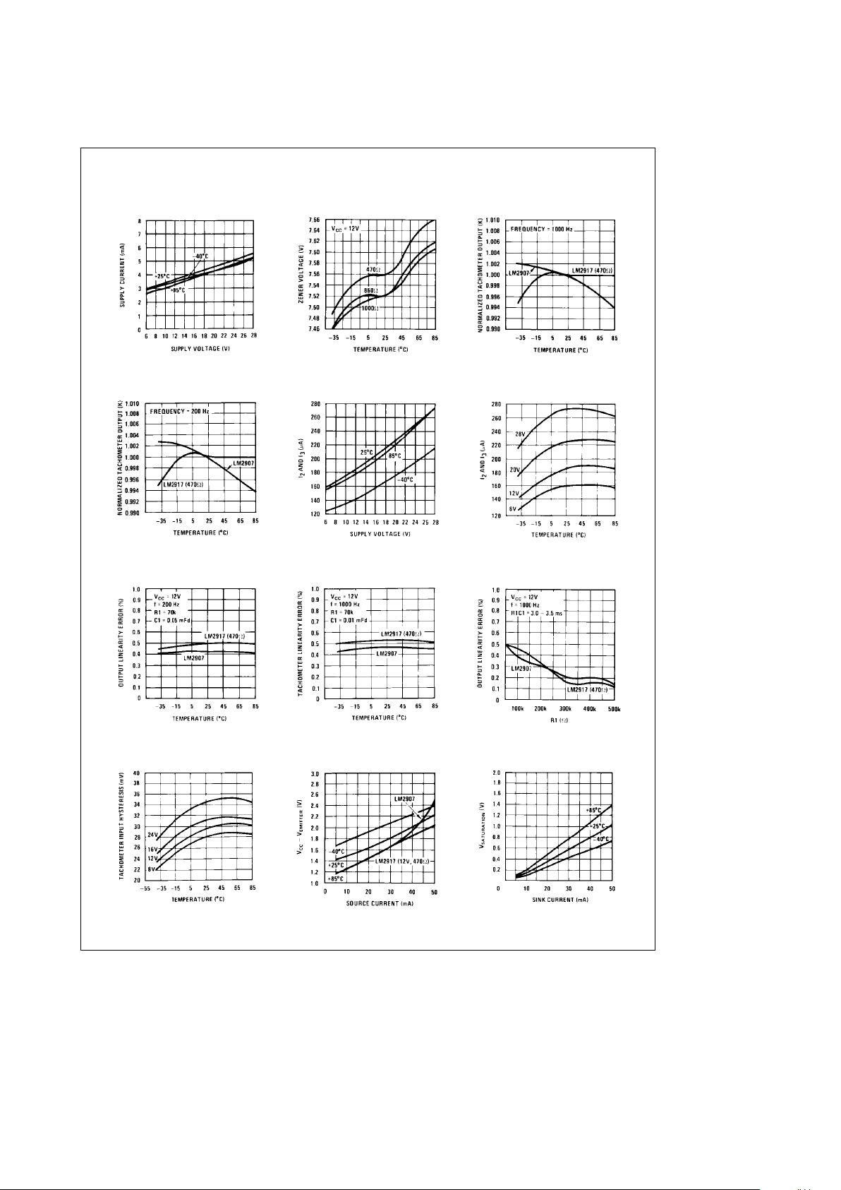
Typical Performance Characteristics
Total Supply Current Temperature
Zener Voltage vs
Output vs Temperature
Normalized Tachometer
Output vs Temperature
Normalized Tachometer
and I
3
vs Supply Voltage
Tachometer Currents I
2
and I3vs Temperature
Tachometer Currents I
2
vs Temperature
Tachometer Linearity
vs Temperature
Tachometer Linearity
Tachometer Linearity vs R1
vs Temperature
Tachometer Input Hysteresis
Characteristics
Op Amp Output Transistor
Characteristics
Op Amp Output Transistor
TL/H/7942– 5
4
Applications Information
The LM2907 series of tachometer circuits is designed for
minimum external part count applications and maximum versatility. In order to fully exploit its features and advantages
let’s examine its theory of operation. The first stage of operation is a differential amplifier driving a positive feedback
flip-flop circuit. The input threshold voltage is the amount of
differential input voltage at which the output of this stage
changes state. Two options (LM2907-8, LM2917-8) have
one input internally grounded so that an input signal must
swing above and below ground and exceed the input
thresholds to produce an output. This is offered specifically
for magnetic variable reluctance pickups which typically provide a single-ended ac output. This single input is also fully
protected against voltage swings to
g
28V, which are easily
attained with these types of pickups.
The differential input options (LM2907, LM2917) give the
user the option of setting his own input switching level and
still have the hysteresis around that level for excellent noise
rejection in any application. Of course in order to allow the
inputs to attain common-mode voltages above ground, input
protection is removed and neither input should be taken
outside the limits of the supply voltage being used. It is very
important that an input not go below ground without some
resistance in its lead to limit the current that will then flow in
the epi-substrate diode.
Following the input stage is the charge pump where the
input frequency is converted to a dc voltage. To do this
requires one timing capacitor, one output resistor, and an
integrating or filter capacitor. When the input stage changes
state (due to a suitable zero crossing or differential voltage
on the input) the timing capacitor is either charged or discharged linearly between two voltages whose difference is
V
CC
/2. Then in one half cycle of the input frequency or a
time equal to 1/2 f
IN
the change in charge on the timing
capacitor is equal to V
CC
/2cC1. The average amount of
current pumped into or out of the capacitor then is:
DQ
T
e
i
c(AVG)
e
C1
c
V
CC
2
c
(2fIN)eV
CC
c
f
IN
c
C1
The output circuit mirrors this current very accurately into
the load resistor R1, connected to ground, such that if the
pulses of current are integrated with a filter capacitor, then
V
O
e
i
c
c
R1, and the total conversion equation becomes:
V
O
e
V
CC
c
f
IN
c
C1cR1cK
Where K is the gain constantÐtypically 1.0.
The size of C2 is dependent only on the amount of ripple
voltage allowable and the required response time.
CHOOSING R1 AND C1
There are some limitations on the choice of R1 and C1
which should be considered for optimum performance. The
timing capacitor also provides internal compensation for the
charge pump and should be kept larger than 500 pF for very
accurate operation. Smaller values can cause an error current on R1, especially at low temperatures. Several considerations must be met when choosing R1. The output current
at pin 3 is internally fixed and therefore V
O
/R1 must be less
than or equal to this value. If R1 is too large, it can become
a significant fraction of the output impedance at pin 3 which
degrades linearity. Also output ripple voltage must be considered and the size of C2 is affected by R1. An expression
that describes the ripple content on pin 3 for a single R1C2
combination is:
V
RIPPLE
e
V
CC
2
c
C1
C2
c
#
1
b
V
CC
c
f
IN
c
C1
I
2
J
pk-pk
It appears R1 can be chosen independent of ripple, however response time, or the time it takes V
OUT
to stabilize at a
new voltage increases as the size of C2 increases, so a
compromise between ripple, response time, and linearity
must be chosen carefully.
As a final consideration, the maximum attainable input frequency is determined by V
CC
, C1 and I2:
f
MAX
e
I
2
C1cV
CC
USING ZENER REGULATED OPTIONS (LM2917)
For those applications where an output voltage or current
must be obtained independent of supply voltage variations,
the LM2917 is offered. The most important consideration in
choosing a dropping resistor from the unregulated supply to
the device is that the tachometer and op amp circuitry alone
require about 3 mA at the voltage level provided by the
zener. At low supply voltages there must be some current
flowing in the resistor above the 3 mA circuit current to operate the regulator. As an example, if the raw supply varies
from 9V to 16V, a resistance of 470X will minimize the zener voltage variation to 160 mV. If the resistance goes under 400X or over 600X the zener variation quickly rises
above 200 mV for the same input variation.
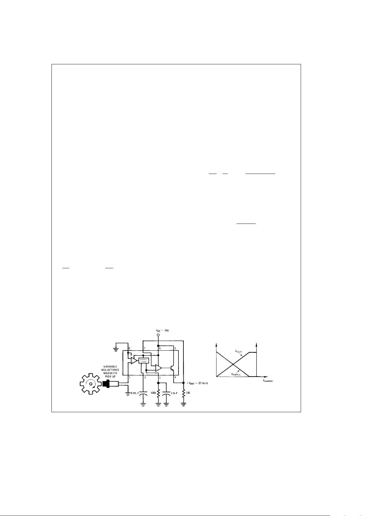
Typical Applications
Minimum Component Tachometer
TL/H/7942– 8
5
Typical Applications (Continued)
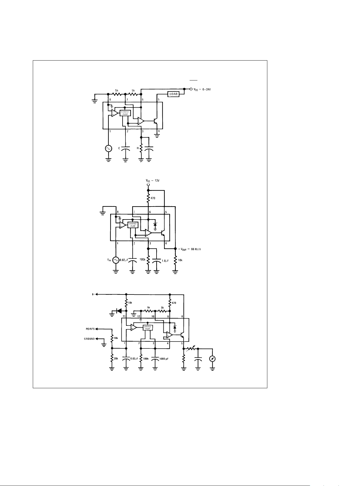
‘‘Speed Switch’’ Load is Energized When f
IN
t
1
2RC
TL/H/7942– 9
Zener Regulated Frequency to Voltage Converter
TL/H/7942– 10
Breaker Point Dwell Meter
TL/H/7942– 11
6
 Loading...