NSC LM2767M5X, LM2767M5 Datasheet

LM2767
Switched Capacitor Voltage Converter
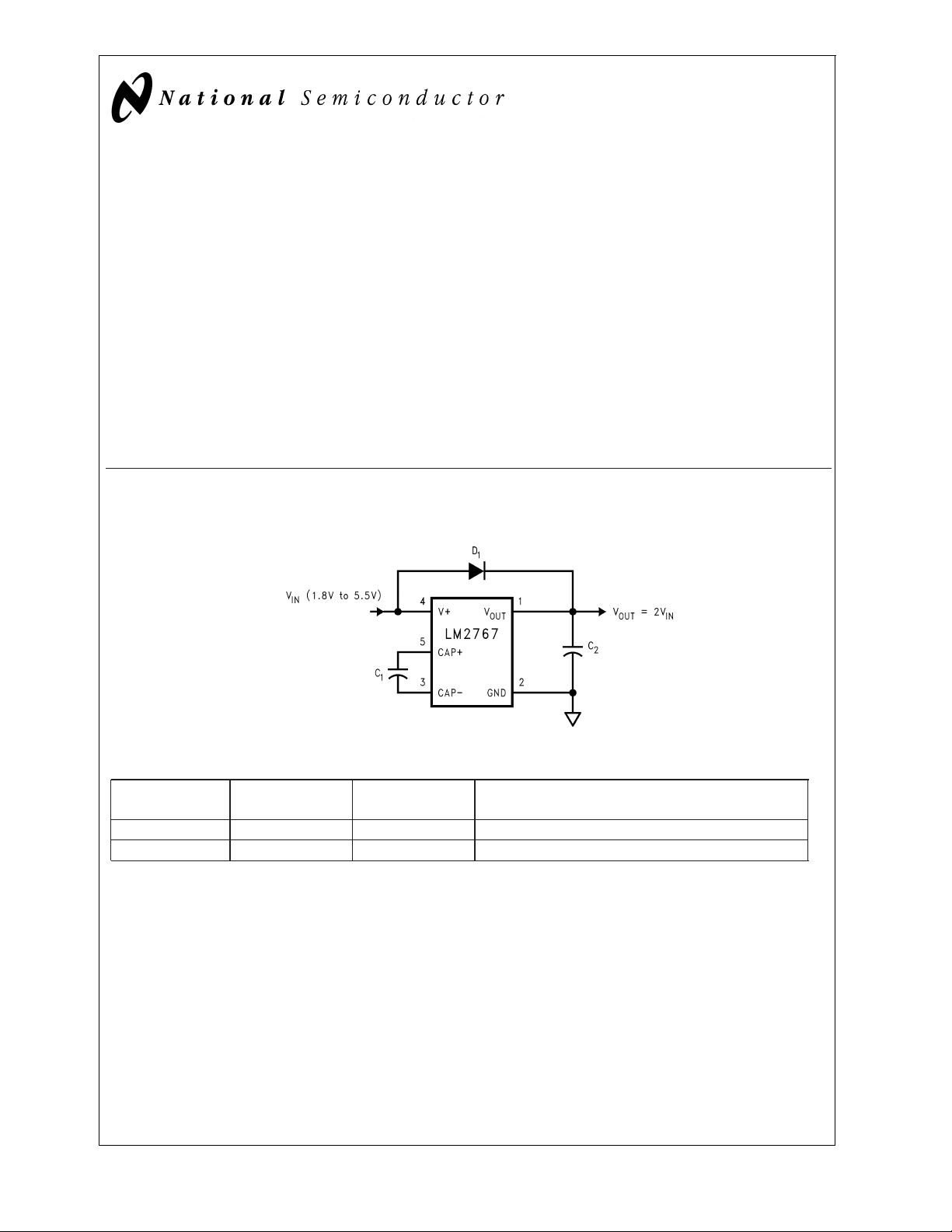
LM2767 Switched Capacitor Voltage Converter
February 2000
General Description
The LM2767 CMOS charge-pump voltage converter operates as a voltage doubler for an input voltage in the range of
+1.8V to +5.5V. Two low cost capacitors and a diode are
used inthiscircuit to provide at least 15 mAof output current.
The LM2767 operates at 11 kHz switching frequency to
avoid audio voice-band interference. With an operating current of only 40 µA (operating efficiency greater than 90%with
most loads), the LM2767 provides ideal performance for battery powered systems. The device is manufactured in a
SOT23-5 package.
Basic Application Circuit
Voltage Doubler
Features
n Doubles Input Supply Voltage
n SOT23-5 Package
n 20Ω Typical Output Impedance
n 96%Typical Conversion Efficiency at 15mA
Applications
n Cellular Phones
n Pagers
n PDAs, Organizers
n Operational Amplifier Power Suppliers
n Interface Power Suppliers
n Handheld Instruments
DS101274-1
Ordering Information
Order Number Package
Number
LM2767M5 MA05B S17B (Note 1) Tape and Reel (1000 units/reel)
LM2767M5X MA05B S17B (Note 1) Tape and Reel (3000 units/reel)
Note 1: The small physical size of the SOT-23 package does not allow for the full part number marking. Devices will be marked with the designation shown in
the column Package Marking.
© 2000 National Semiconductor Corporation DS101274 www.national.com
Package
Marking
Supplied as

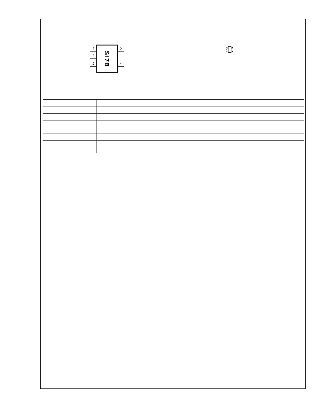
Connection Diagram
LM2767
Top View With Package Marking
Pin Description
Pin Name Function
1V
2 GND Power supply ground input.
3 CAP− Connect this pin to the negative terminal of the
4 V+ Power supply positive voltage input.
5 CAP+ Connect this pin to the positive terminal of the
DS101274-13
OUT
5-Lead SOT (M5)
DS101274-22
Actual Size
Positive voltage output.
charge-pump capacitor.
charge-pump capacitor.
www.national.com 2

LM2767
Absolute Maximum Ratings (Note 2)
If Military/Aerospace specified devices are required,
please contact the National Semiconductor Sales Office/
Distributors for availability and specifications.
Supply Voltage (V+ to GND, or V+ to V
V
Continuous Output Current 30 mA
OUT
Output Short-Circuit Duration to GND (Note 3) 1 sec.
Continuous Power
Dissipation (T
T
(Note 4) 150˚C
JMax
=
25˚C)(Note 4)
A
) 5.8V
OUT
400 mW
Operating Ratings
θJA(Note 4) 210˚C/W
Junction Temperature Range −40˚C to 100˚C
Ambient Temperature Range −40˚C to 85˚C
Storage Temperature Range −65˚C to 150˚C
Lead Temp. (Soldering, 10 sec.) 240˚C
ESD Rating (Note 5)
Human Body Model
Machine Model
200V
2kV
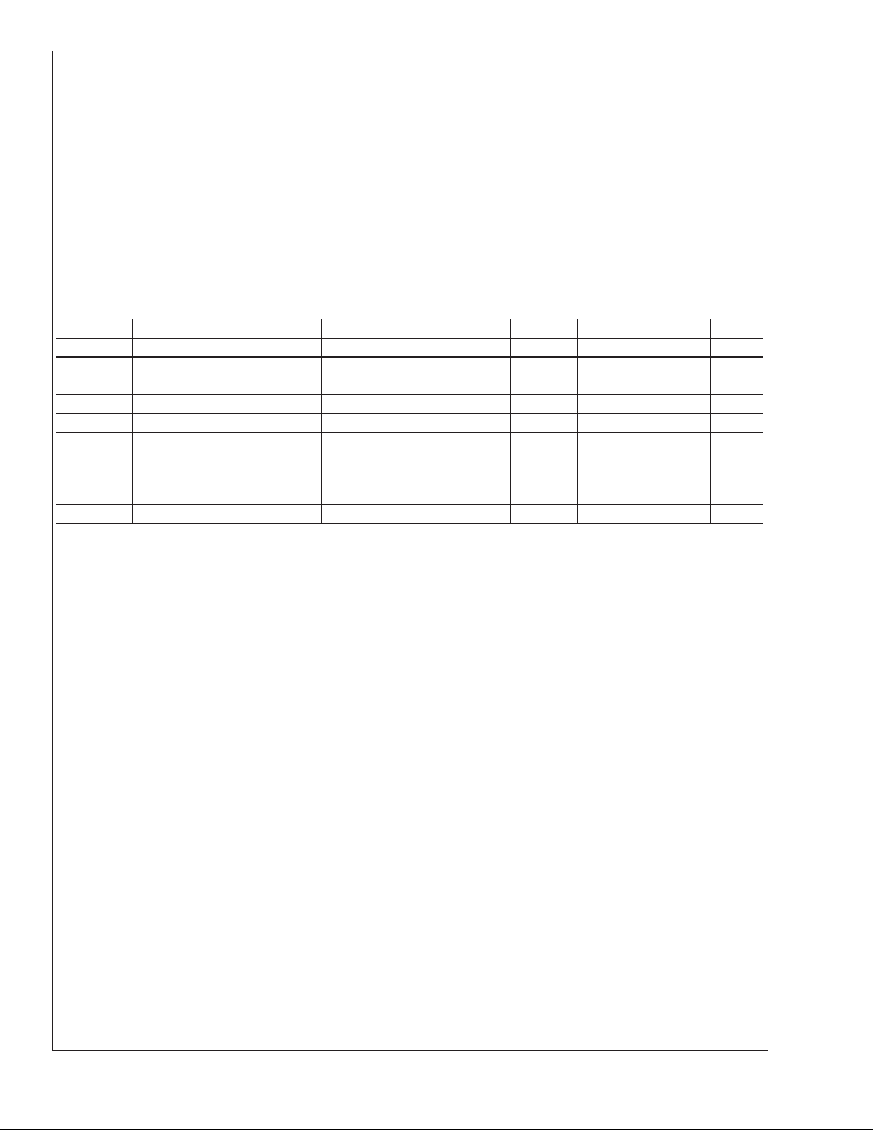
Electrical Characteristics
Limits in standard typeface are for T
less otherwise specified: V+=5V, C
Symbol Parameter Condition Min Typ Max Units
V+ Supply Voltage 1.8 5.5 V
I
Q
I
L
R
OUT
f
OSC
f
SW
P
EFF
V
OEFF
Note 2: Absolute maximum ratings indicate limits beyond which damage to the device may occur. Electrical specifications do not apply when operating the device
beyond its rated operating conditions.
Note 3: V
Note 4: The maximum allowable power dissipation is calculated by using P
ambient temperature, and θ
Note 5: The human body model is a 100pF capacitor discharged through a 1.5kΩ resistor into each pin. The machine model is a 200pF capacitor discharged directly
into each pin.
Note 6: In thetest circuit, capacitors C
voltage and efficiency.
Note 7: Specified output resistance includes internal switch resistance and capacitor ESR. See the details in the application information for positive voltage doubler.
Note 8: The output switches operate at one half of the oscillator frequency, f
Supply Current No Load 40 90 µA
Output Current 1.8V ≤ V+ ≤ 5.5V 15 mA
Output Resistance (Note 7) I
Oscillator Frequency (Note 8) 8 22 50 kHz
Switching Frequency (Note 8) 4 11 25 kHz
Power Efficiency RL(5.0k) between GND and
Voltage Conversion Efficiency No Load 99.96
may be shorted toGND for one second without damage. For temperatures above 85˚C, V
OUT
is the junction-to-ambient thermal resistance of the specified package.
JA
=
25˚C, and limits in boldface type apply over the full operating temperature range. Un-
J
=
=
C
1
and C2are 10 µF,0.3Ω maximum ESR capacitors. Capacitors with higher ESR will increase output resistance, reduce output
1
10 µF. (Note 6)
2
L
OUT
I
L
=
15 mA 20 40 Ω
98
=
15 mA to GND 96
must not be shortedto GND or device may be damaged.
OUT
)/θJA, where T
is the maximum junction temperature, TAis the
JMax
DMax
OSC
=
(T
=
2f
JMax−TA
.
SW
%
%
www.national.com3
 Loading...