

NSC LM2724ALD, LM2724AMX, LM2724AM, LM2724ALDX Datasheet
LM2724A
High Speed 3A Synchronous MOSFET Driver
General Description
The LM2724A is a dual N-channel MOSFET driver which
can drive both the top and bottom MOSFETs in a push-pull
structure simultaneously. The LM2724A takes a logic input
and splits it into two complimentary signals with a typical
20ns dead time in between. The built-in cross-conduction
protection circuitry prevents the top and bottom MOSFETs
from turning on simultaneously. With a bias voltage of 5V, the
peak sourcing and sinking current for each driver of the
LM2724A is about 3A. Input UVLO (Under-Voltage-LockOut) ensures that all the driver outputs stay low until the
supply rail exceeds the power-on threshold during system
power on, or after the supply rail drops below power-on
threshold by a specified hysteresis during system power
down. The cross-conduction protection circuitry detects both
driver outputs and will not turn on a driver until the other
driver output is low. The top gate voltage needed by the top
MOSFET is obtained through an external boot-strap structure. When not switching, the LM2724A only draws up to
195µA from the 5V rail. The synchronization operation of the
bottom MOSFET can be disabled by pulling the SYNC pin to
ground.
Features
n Shoot-through protection
n Input Under-Voltage-Lock-Out
n 3A peak driving current
n 195µA quiescent current
n 28V input voltage in buck configuration
n SO-8 and LLP packages
Applications
n High Current DC/DC Power Supplies
n High Input Voltage Switching Regulators
n Fast Transient Microprocessors
n Notebook Computers
LM2724A High Speed 3A Synchronous MOSFET Driver
June 2003
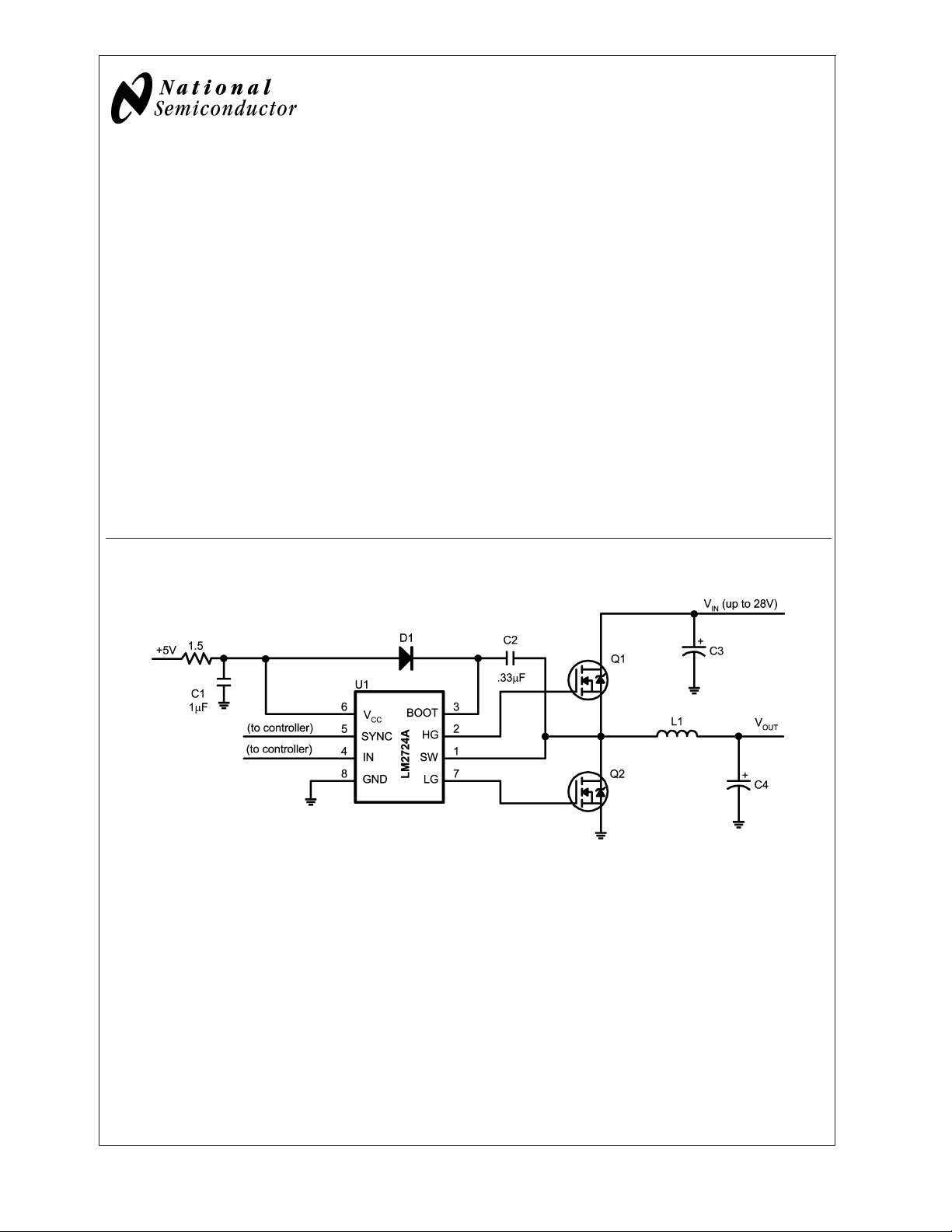
Typical Application
20073501
© 2003 National Semiconductor Corporation DS200735 www.national.com
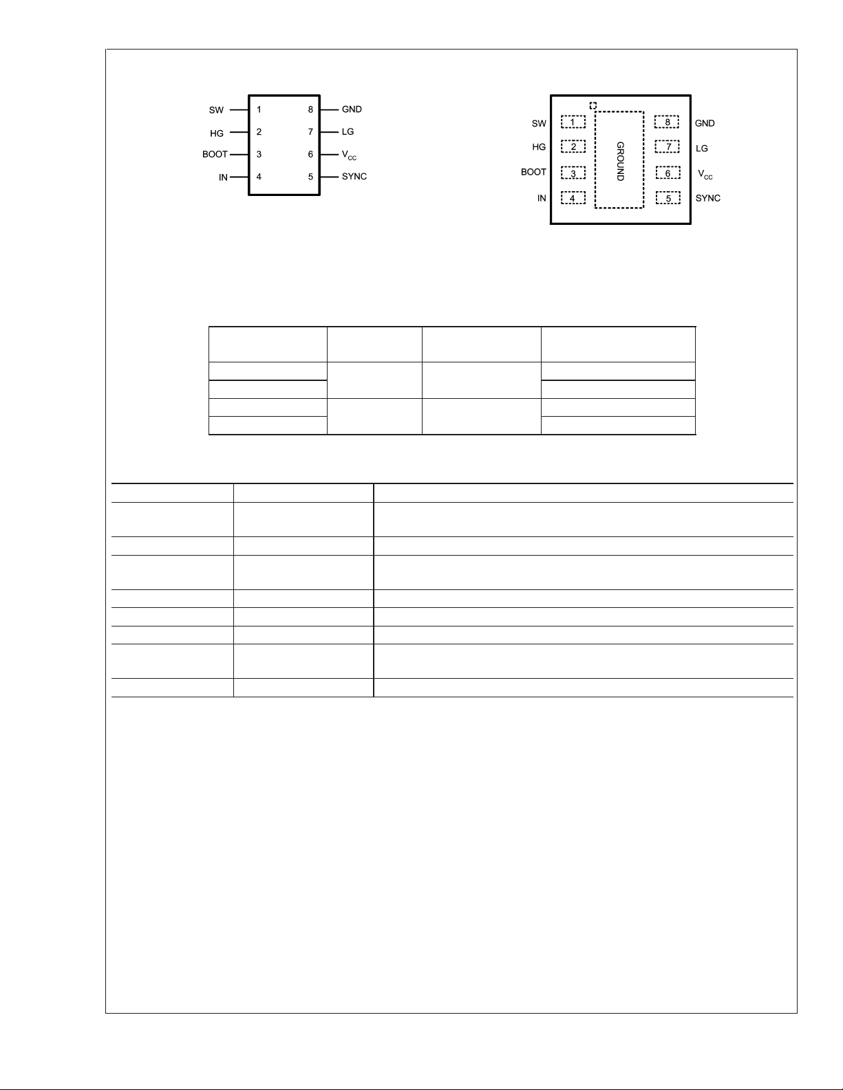
Connection Diagram
LM2724A
8-Lead SO (NS Package # M08A)
20073502
= 172˚C/W
θ
JA
8-Lead LLP (NS Package # LDC08A)
Ordering Information
Order Number Size NSC Package
Drawing
LM2724AM SO-8 M08A 95 Units/Rail
LM2724AMX 2500 Units/Reel
LM2724ALD LDC08A LDC08A 1000 Units/Rail
LM2724ALDX 4500 Units/Reel
Pin Descriptions
Pin Name Function
1SW
2 HG Top gate drive output. Should be connected to the top FET gate.
3 BOOT
4 IN Accepts a logic control signal
5 SYNC Bottom gate enable
6V
CC
7LG
8 GND Ground
Top driver return. Should be connected to the common node of top
and bottom FETs
Bootstrap. Accepts a bootstrap voltage for powering the high-side
driver
Connect to +5V supply
Bottom gate drive output. Should be connected to the bottom FET
gate.
= 39˚C/W
θ
JA
Supplied As
20073506
www.national.com 2
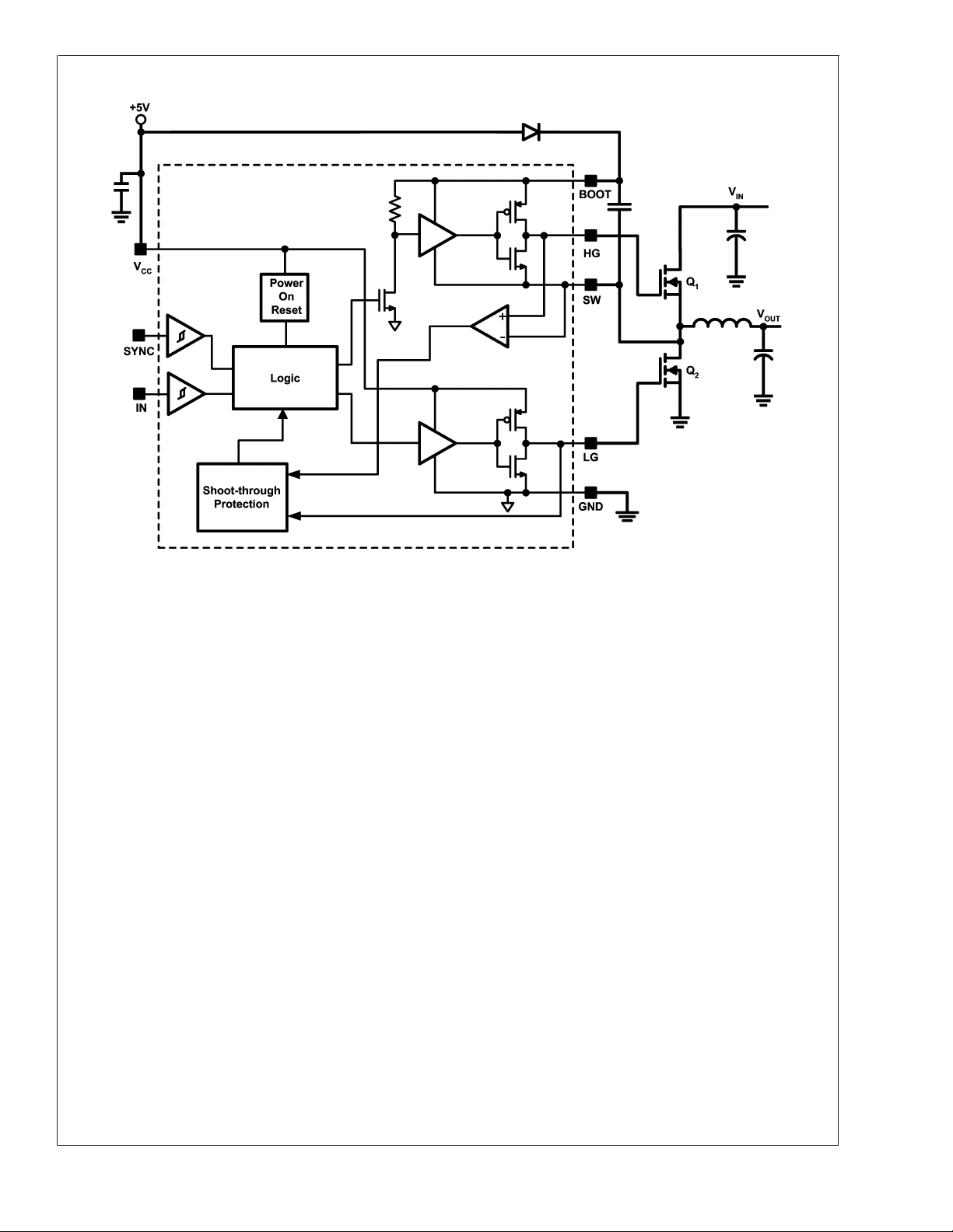
Block Diagram
LM2724A
20073503
www.national.com3
 Loading...