

NSC LM2711MTX-ADJ, LM2711MT-ADJ Datasheet
LM2711
TFT Panel Module
LM2711 TFT Panel Module
July 2003
General Description
The LM2711 is a compact bias solution for TFT displays. It
has a current mode PWM step-up DC/DC converter with a
1.4A, 0.17Ω internal switch. Capable of generating 8V at
300mA from a Lithium Ion battery, the LM2711 is ideal for
generating bias voltages for large screen LCD panels. The
LM2711 can be operated at switching frequencies of 600kHz
or 1.25MHz, allowing for easy filtering and low noise. An
external compensation pin gives the user flexibility in setting
frequency compensation, which makes possible the use of
small, low ESR ceramic capacitors at the output. The
LM2711 uses a patented internal circuitry to limit startup
inrush current of the boost switching regulator without the
use of an external softstart capacitor. An external softstart
pin enables the user to tailor the softstart to a specific
application. The LM2711 contains 4 Gamma buffers capable
of supplying 50mAsource and sink. The TSSOP-20 package
ensures a low profile overall solution.
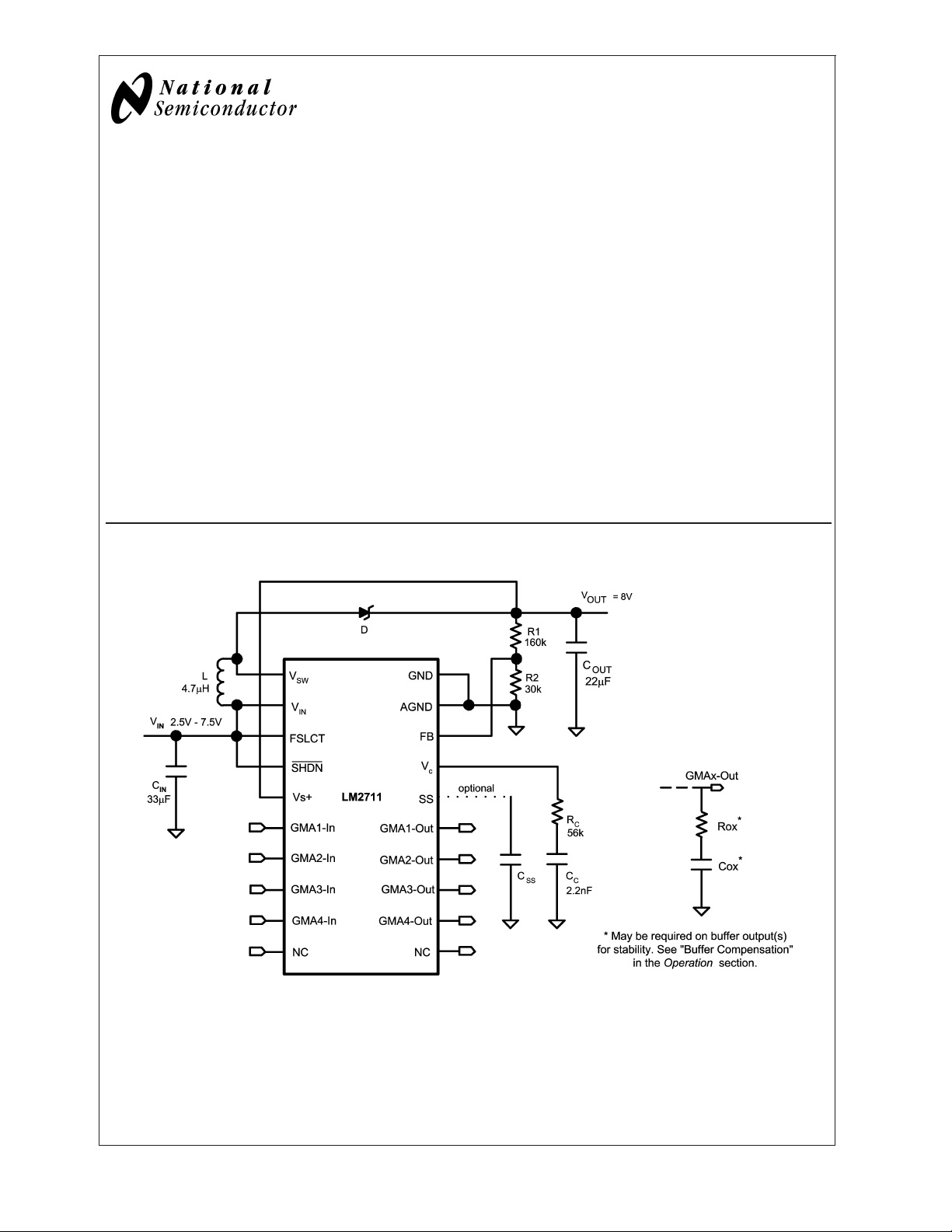
Typical Application Circuit
Features
n 1.4A, 0.17Ω, internal power switch
n V
operating range: 2.2V to 7.5V
IN
n 600kHz/1.25MHz selectable frequency step-up DC/DC
converter
n 20 pin TSSOP package
n Inrush current limiting circuitry
n External softstart override
n 4 Gamma buffers
Applications
n LCD Bias Supplies
20046831
© 2003 National Semiconductor Corporation DS200468 www.national.com
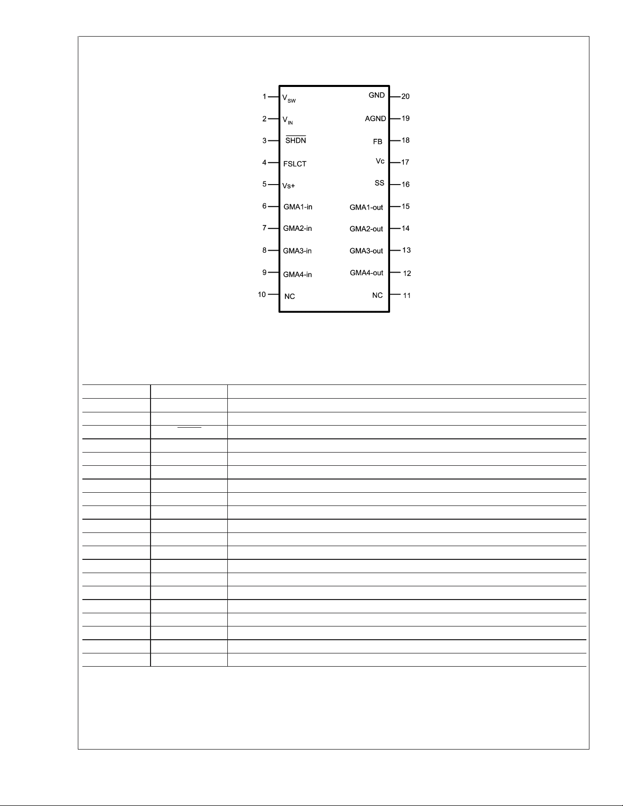
Connection Diagram
LM2711
Top View
TSSOP 20 package
20046804
= 125˚C, θJA= 120˚C/W (Note 1)
T
JMAX
Pin Description
Pin Name Function
1V
2V
SW
IN
3 SHDN
4 FSLCT Frequency Select pin. FSLCT = V
5 Vs+ Gamma Buffer input supply.
6 GMA1-in Gamma Buffer input.
7 GMA2-in Gamma Buffer input.
8 GMA3-in Gamma Buffer input.
9 GMA4-in Gamma Buffer input.
10 NC No Connection, leave open.
11 NC No Connection, leave open.
12 GMA4-out Gamma Buffer output.
13 GMA3-out Gamma Buffer output.
14 GMA2-out Gamma Buffer output.
15 GMA1-out Gamma Buffer output.
16 SS Soft start pin.
17 V
C
18 FB Output Voltage Feedback input.
19 AGND Gamma Buffer ground, Analog ground connection for Regulator.
20 GND Switch Power Ground.
Power switch input.
Switching Regulator Power input.
Shutdown pin, active low.
for 1.25 MHz, FSLCT = AGND or floating for 600kHz.
IN
Boost Compensation Network Connection.
www.national.com 2

Pin Functions
VSW(Pin 1): This is the drain of the internal NMOS power
switch. Minimize the metal trace area connected to this pin to
minimize EMI.
(Pin 2): Input Supply Pin. Bypass this pin with a capacitor
V
IN
as close to the device as possible. The capacitor should
connect between V
SHDN(Pin 3): Shutdown Pin. The shutdown pin signal is
active low. A voltage of less than 0.3V disables the device. A
voltage greater than 0.85V enables the device.
FSLCT(Pin 4): Frequency Select Pin. Connecting FSLCT to
AGND selects a 600 kHz operating frequency for the switching regulator. Connecting FSLCT to V
operating frequency. If FSLCT is left floating, the switching
frequency defaults to 600 kHz.
Vs+(Pin 5): Supply pin for the four Gamma buffers. Bypass
this pin with a capacitor as close to the device as possible.
The capacitor should connect between Vs+ and GND.
GMA1-in(Pin 6):Gamma Buffer input pin.
GMA2-in(Pin 7): Gamma Buffer input pin.
GMA3-in(Pin 8): Gamma Buffer input pin.
GMA4-in(Pin 9): Gamma Buffer input pin.
NC(Pin 10):No Connection.
NC(Pin 11): No Connection.
and GND.
IN
selects a 1.25 MHz
IN
GMA4-out(Pin 12): Gamma Buffer output pin.
GMA3-out(Pin13): Gamma Buffer output pin.
GMA2-out(Pin 14): Gamma Buffer output pin.
GMA1-out(Pin 15): Gamma Buffer output pin.
SS(Pin 16): Softstart pin. Connect capacitor to SS pin and
AGND to slowly ramp inductor current on startup.
(Pin 17): Compensation Network for Boost switching
V
C
regulator. Connect resistor/capacitor network between V
pin and AGND for boost switching regulator AC compensation.
FB(Pin 18): Feedback pin. Set the output voltage by selecting values of R1 and R2 using:
Connect the ground of the feedback network to the AGND
plane, which can be tied directly to the GND pin.
AGND(Pin 19): Analog ground pin. Ground connection for
the Gamma buffers and the boost switching regulator. AGND
must be tied directly to GND at the pins.
GND(Pin 20): Power ground pin. Ground connection for the
NMOS power device of the boost switching regulator. GND
must be tied directly to AGND at the pins.
LM2711
C
Ordering Information
Order Number Package Type NSC Package Drawing Supplied As
LM2711MT-ADJ TSSOP-20 MTC20 73 Units, Rail
LM2711MTX-ADJ TSSOP-20 MTC20 2500 Units, Tape and Reel
www.national.com3

Block Diagrams
LM2711
20046803
20046851
www.national.com 4
LM2711
Absolute Maximum Ratings (Note 2)
If Military/Aerospace specified devices are required,
please contact the National Semiconductor Sales Office/
Distributors for availability and specifications.
V
IN
V
Voltage -0.3V to 18V
SW
-0.3V to 7.5V
ESD Ratings
(Note 3)
Human Body Model 2kV
Machine Model 200V
Operating Conditions
FB Voltage -0.3V to 7V
V
Voltage 0.965V to 1.565V
C
SHDN Voltage
-0.3V to V
FSLCT Voltage AGND to V
Supply Voltage, Vs+ -0.3V to 12V
Buffer Input Voltage Rail-to-Rail
IN
IN
Operating Temperature −40˚C to +125˚C
Storage Temperature −65˚C to +150˚C
Supply Voltage, V
V
Voltage 17V
SW
IN
2.2V to 7.5V
Supply Gamma Buffer, Vs+ 4V to 12V
Buffer Output Voltage Rail-to-Rail
Electrical Characteristics
Specifications in standard type face are for TJ= 25˚C and those with boldface type apply over the full Operating Temperature Range (T
Switching Regulator
Symbol Parameter Conditions
I
Q
V
FB
%V
/∆VINFeedback Voltage Line
FB
I
CL
R
DSON
I
B
V
IN
I
SS
T
SS
g
m
A
V
D
MAX
f
S
I
L
SHDN
I
SHDN
UVP On Threshold 1.8 1.9 2 V
= −40˚C to +125˚C). Unless otherwise specified, VIN=2.2V and Vs+ = 8V, Rox = 50Ω, Cox = 1nF.
J
Min
(Note 4)
Typ
(Note 5)
Max
(Note 4)
Units
Quiescent Current Not Switching, FSCLT = 0V 1.6 2
Not Switching, FSCLT = V
IN
Switching, FSCLT = 0V 2.5 3
Switching, FSCLT = V
IN
1.65 2.2
3.4 4
mA
Shutdown mode 6 15 µA
Feedback Voltage 1.239 1.265 1.291 V
Regulation
Switch Current Limit
(Note 6)
Switch R
(Note 7) VIN= 2.7V 170 mΩ
DSON
VIN= 2.5V, V
OUT
=8V
0.03 0.05 %/V
1.4 A
FB Pin Bias Current(Note 8) 30 90 nA
Input Voltage Range 2.2 7.5 V
Soft Start Current 5 11 15 µA
Internal Soft Start Ramp
Time
FSLCT = 0V
6.7 10 mS
Error Amp Transconductance ∆I = 5µA 60 135 250 µmho
Error Amp Voltage Gain 135 V/V
Maximum Duty Cycle 78 85 %
Switching Frequency FSLCT = 0V 500 600 700 kHz
FSLCT = V
IN
0.9 1.25 1.5 MHz
Switch Leakage Current VSW= 17V 0.185 20 µA
SHDN Threshold Output High 0.85 0.6 V
Output Low 0.6 0.3 V
Shutdown Pin Current 0V ≤ SHDN ≤ V
IN
0.5 1 µA
Off Threshold 1.7 1.8 1.9 V
Hysteresis 100 mV
www.national.com5
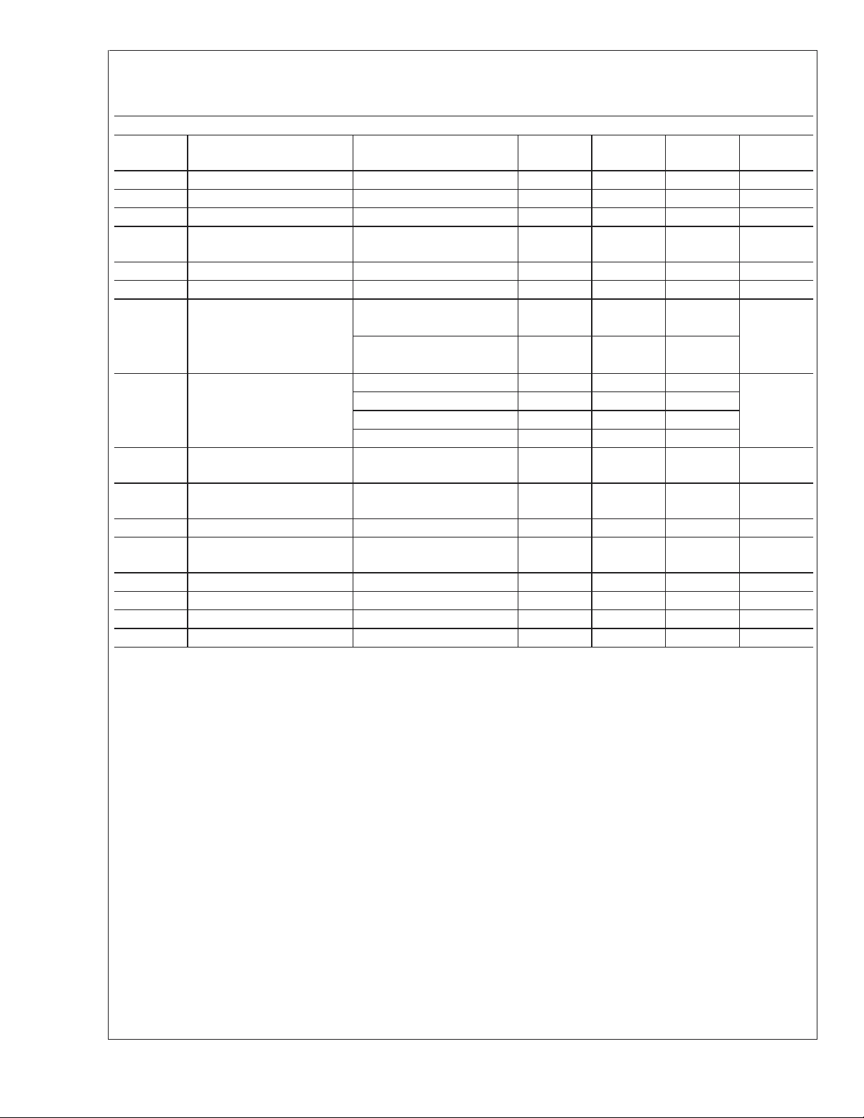
Electrical Characteristics
Specifications in standard type face are for TJ= 25˚C and those with boldface type apply over the full Operating Tempera-
LM2711
ture Range (T
BUFFERS
Symbol Parameter Conditions
V
OS
∆V
/∆T Offset Voltage Drift 8 µV/˚C
os
I
B
CMVR Input Common-mode Voltage
Z
IN
C
IN
I
OUT
V
Swing RL=10k, Vo min. 0.075
OUT
A
VCL
NL Gain Linearity R
Vs+ Supply Voltage 412V
PSRR Power Supply Rejection
Is+ Supply Current/Amplifier Vo = Vs+/2, No Load 1 2 mA
SR Slew Rate 10 V/µs
BW Bandwidth -3dB,R
φ 0 Phase Margin 50 Deg˚
Note 1: The maximum allowable power dissipation is a function of the maximum junction temperature, TJ(MAX), the junction-to-ambient thermal resistance, θJA,
and the ambient temperature, T
at any ambient temperature is calculated using: P
temperature, and the regulator will go into thermal shutdown.
Note 2: Absolute maximum ratings are limits beyond which damage to the device may occur. Operating Ratings are conditions for which the device is intended to
be functional, but device parameter specifications may not be guaranteed. For guaranteed specifications and test conditions, see the Electrical Characteristics.
Note 3: The human body model is a 100 pF capacitor discharged through a 1.5kΩ resistor into each pin. The machine model is a 200pF capacitor discharged
directly into each pin.
Note 4: All limits guaranteed at room temperature (standard typeface) and at temperature extremes (bold typeface). All room temperature limits are 100%
production tested or guaranteed through statistical analysis. All limits at temperature extremes are guaranteed via correlation using standard Statistical Quality
Control (SQC) methods. All limits are used to calculate Average Outgoing Quality Level (AOQL).
Note 5: Typical numbers are at 25˚C and represent the most likely norm.
Note 6: Duty cycle affects current limit due to ramp generator. See Switch Current Limit vs. V
Performance Characteristics section.
Note 7: See Typical Performance Characteristics section for Tri-Temperature data for R
Note 8: Bias current flows into FB pin.
= −40˚C to +125˚C). Unless otherwise specified, VIN=2.2V and Vs+ = 8V, Rox = 50Ω, Cox = 1nF.
J
Min
(Note 4)
Typ
(Note 5)
Max
(Note 4)
Input offset voltage 2.5 10 mV
Input Bias Current 170 800 nA
Range
0.05 Vs+-0.05 V
Input Impedance 400 kΩ
Input Capacitance 1 pF
Continuous Output Current Vs+=8V, Source 41 59 71
Vs+=8V, Sink −65 −53 −36
Vs+=12V, Source 50 71 85
Vs+=12V, Sink −75 −61 −42
R
=10k, Vo max. 7.88
L
R
=2k, Vo min. 0.075
L
R
=2k, Vo max. 7.865
L
Voltage Gain RL=2 kΩ
=10 kΩ
R
L
=2 kΩ, Buffer input=0.5 to
L
(Vs+-0.5V)
Vs+=4to12V
Ratio
L
. See the Electrical Characteristics table for the thermal resistance of various layouts. The maximum allowable power dissipation
A
(MAX) = (T
D
0.995
0.9985
=10 kΩ,CL=10pf 6 MHz
J(MAX)−TA
)/θJA. Exceeding the maximum allowable power dissipation will cause excessive die
and Switch Current Limit vs. Temperature graphs in the Typical
IN
vs. VIN.
DSON
0.998
0.9999
0.01 %
90 316 µV/V
Units
mA
V
V/V
www.national.com 6
 Loading...