

LM2642
Two-Phase Synchronous Step-Down Switching
Controller
General Description
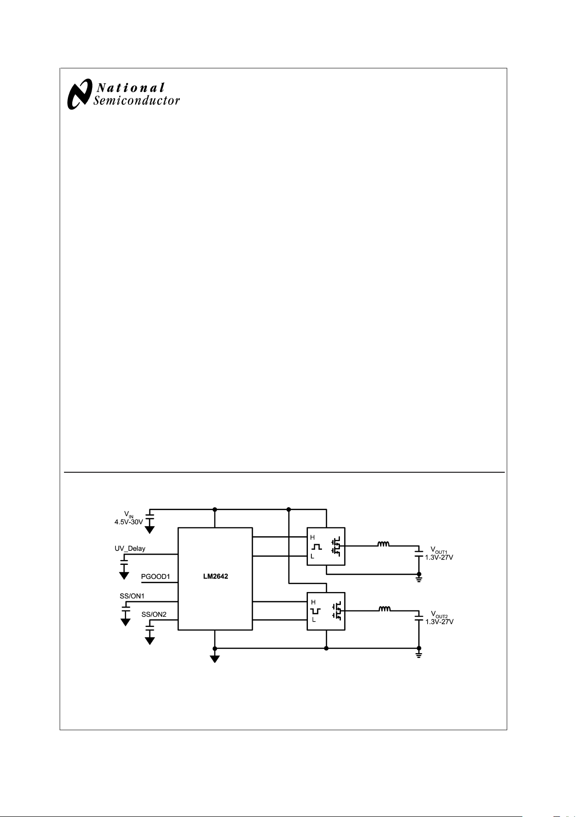
The LM2642 consists of two current mode synchronous
buck regulator controllers with a switching frequency of
300kHz.
The two switching regulator controllers operate 180˚ out of
phase. This feature reduces the input ripple RMS current,
thereby significantly reducing the required input capacitance.
The two switching regulator outputs can also be paralleled to
operate as a dual-phase single output regulator.
The output of each channel can be independently adjusted
from 1.3 to V
IN
•
maximum duty cycle. An internal 5V rail is
also available externally for driving bootstrap circuitry.
Current-mode feedback control assures excellent line and
load regulation and a wide loop bandwidth for excellent
response to fast load transients. Current is sensed across
either the Vds of the top FET or across an external currentsense resistor connected in series with the drain of the top
FET. Current limit is independently adjustable for each channel.
The LM2642 features analog soft-start circuitry that is independent of the output load and output capacitance. This
makes the soft-start behavior more predictable and controllable than traditional soft-start circuits.
A PGOOD1 pin is provided to monitor the dc output of
channel 1. Over-voltage protection is available for both outputs. A UV-Delay pin is also available to allow delayed shut
off time for the IC during an output under-voltage event.
Features
n Two synchronous buck regulators
n 180˚ out of phase operation
n 4.5V to 30V input range
n Power good function monitors Ch.1
n 37µA Shutdown current
n 0.04% (typical) line and load regulation error
n Current mode control with or without a sense resistor
n Independent enable/soft-start pins allow simple
sequential startup configuration.
n Configurable for single output parallel operation. (See
Figure 2).
n Adjustable cycle-by-cycle current limit
n Input under-voltage lockout
n Output over-voltage latch protection
n Output under-voltage protection with delay
n Thermal shutdown
n Self discharge of output capacitors when the regulator is
OFF
n TSSOP package
Applications
n Embedded computer systems
n High end gaming systems
n Set-top boxes
n WebPAD
Block Diagram
20046201
May 2003
LM2642 Two-Phase Synchronous Step-Down Switching Controller
© 2003 National Semiconductor Corporation DS200462 www.national.com
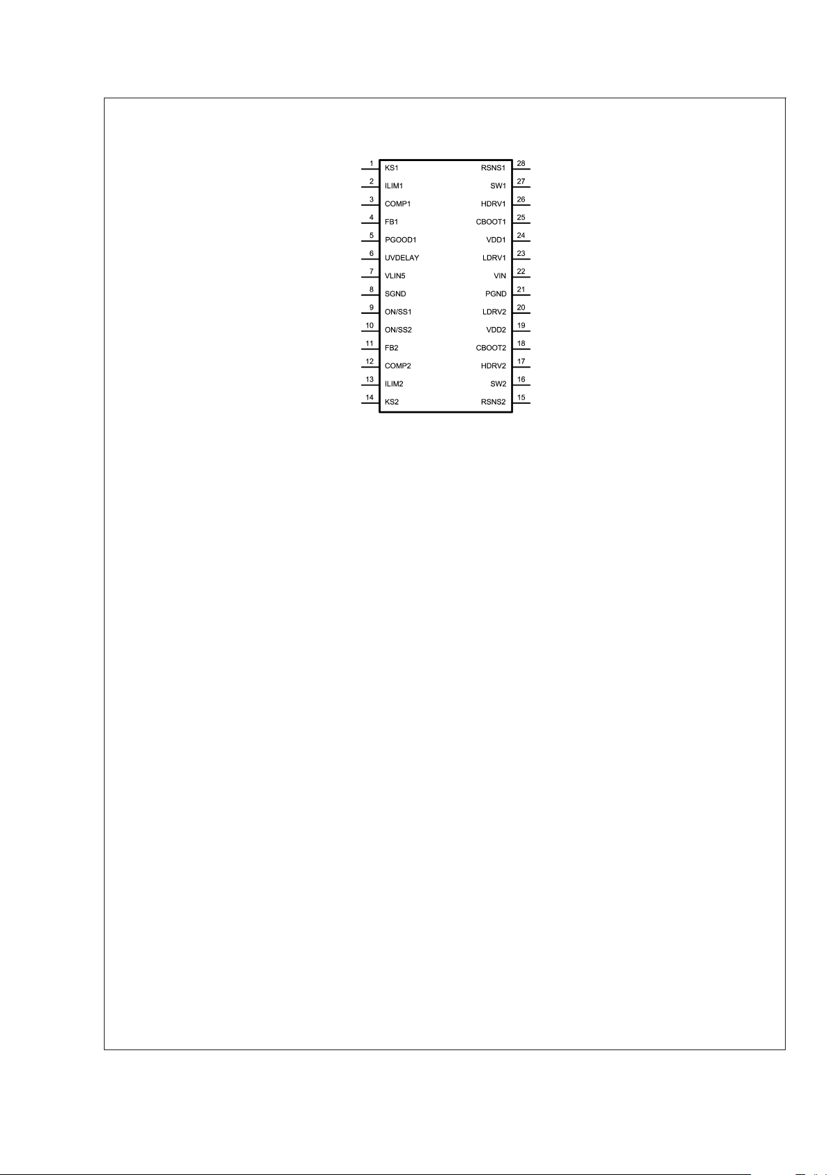
Connection Diagram
TOP VIEW
20046202
28-Lead TSSOP (MTC)
Order Number LM2642MTC
See NS Package Number MTC28
Pin Descriptions
KS1 (Pin 1): The positive (+) Kelvin sense for the internal
current sense amplifier of Channel 1. Use a separate trace to
connect this pin to the current sense point. It should be
connected to VIN as close as possible to the node of the
current sense resistor. When no current-sense resistor is
used, connect as close as possible to the drain node of the
upper MOSFET.
ILIM1 (Pin 2): Current limit threshold setting for Channel 1. It
sinks a constant current of 10 µA, which is converted to a
voltage across a resistor connected from this pin to VIN. The
voltage across the resistor is compared with either the VDS
of the top MOSFET or the voltage across the external current sense resistor to determine if an over-current condition
has occurred in Channel 1.
COMP1 (Pin 3): Compensation pin for Channel 1. This is the
output of the internal transconductance amplifier. The compensation network should be connected between this pin
and the signal ground, SGND (Pin 8).
FB1 (Pin 4): Feedback input for channel 1. Connect to
VOUT through a voltage divider to set the channel 1 output
voltage.
PGOOD1 (Pin 5): An open-drain power-good output for
Channel 1. It is ’LOW’ (low impedance to ground) whenever
the output voltage of Channel 1 falls outside of a +15% to
-9% window. PGOOD1 stays latched in a ’LOW’ state during
OVP or UVP on either channel. It will recover to a ’HIGH’
state (high impedance to ground) after a Channel 1 output
under-voltage event (
<
91%) when the output returns to
within 6% of its nominal value. See Operation Descriptions
for details.
UV_DELAY (Pin 6): A capacitor from this pin to ground sets
the delay time for UVP. The capacitor is charged from a 5µA
current source. When UV_DELAY charges to 2.3V (typical),
the system immediately latches off. Connecting this pin to
ground will disable the output under-voltage protection.
VLIN5 (Pin 7): The output of an internal 5V LDO regulator
derived from VIN. It supplies the internal bias for the chip and
supplies the bootstrap circuitry for gate drive. Bypass this pin
to signal ground with a minimum of 4.7µF capacitor.
SGND (Pin 8): The ground connection for the signal-level
circuitry. It should be connected to the ground rail of the
system.
ON/SS1 (Pin 9): Channel 1 enable pin. This pin is internally
pulled up to one diode drop above VLIN5. Pulling this pin
below 1.2V (open-collector type) turns off Channel 1. If both
ON/SS1 and ON/SS2 pins are pulled below 1.2V, the whole
chip goes into shut down mode. Adding a capacitor to this
pin provides a soft-start feature that minimizes inrush current
and output voltage overshoot.
ON/SS2 (Pin 10): Channel 2 enable pin. See the description
for Pin 9, ON/SS1. May be connected to ON/SS1 for simultaneous startup or for parallel operation.
FB2 (Pin 11): Feedback input for channel 2. Connect to
VOUT through a voltage divider to set the Channel 2 output
voltage.
COMP2 (Pin 12): Compensation pin for Channel 2. This is
the output of the internal transconductance amplifier. The
compensation network should be connected between this
pin and the signal ground SGND (Pin 8).
ILIM2 (Pin 13): Current limit threshold setting for Channel 2.
See ILIM1 (Pin 2).
KS2 (Pin 14): The positive (+) Kelvin sense for the internal
current sense amplifier of Channel 2. See KS1 (Pin 1).
RSNS2 (Pin 15): The negative (-) Kelvin sense for the
internal current sense amplifier of Channel 2. Connect this
pin to the low side of the current sense resistor that is placed
between VIN and the drain of the top MOSFET. When the
Rds of the top MOSFET is used for current sensing, connect
this pin to the source of the top MOSFET. Always use a
separate trace to form a Kelvin connection to this pin.
LM2642
www.national.com 2

Pin Descriptions (Continued)
SW2 (Pin 16): Switch-node connection for Channel 2, which
is connected to the source of the top MOSFET of Channel 2.
It serves as the negative supply rail for the top-side gate
driver, HDRV2.
HDRV2 (Pin 17): Top-side gate-drive output for Channel 2.
HDRV is a floating drive output that rides on the corresponding switching-node voltage.
CBOOT2 (Pin 18): Bootstrap capacitor connection. It serves
as the positive supply rail for the Channel 2 top-side gate
drive. Connect this pin to VDD2 (Pin 19) through a diode,
and connect the low side of the bootstrap capacitor to SW2
(Pin16).
VDD2 (Pin 19): The supply rail for the Channel 2 low-side
gate drive. Connected to VLIN5 (Pin 7) through a 4.7Ω
resistor and bypassed to power ground with a ceramic capacitor of at least 1µF. Tie this pin to VDD1 (Pin 24).
LDRV2 (Pin 20): Low-side gate-drive output for Channel 2.
PGND (Pin 21): The power ground connection for both
channels. Connect to the ground rail of the system.
VIN (Pin 22): The power input pin for the chip. Connect to
the positive (+) input rail of the system. This pin must be
connected to the same voltage rail as the top FET drain (or
the current sense resistor when used).
LDRV1 (Pin 23): Low-side gate-drive output for Channel 1.
VDD1 (Pin 24): The supply rail for Channel 1 low-side gate
drive. Tie this pin to VDD2 (Pin 19).
CBOOT1 (Pin 25): : Bootstrap capacitor connection. It
serves as the positive supply rail for Channel 1 top-side gate
drive. See CBOOT2 (Pin 18).
HDRV1 (Pin 26): Top-side gate-drive output for Channel 1.
See HDRV2 (Pin 17).
SW1 (Pin 27): Switch-node connection for Channel 1. See
SW2 (Pin16).
RSNS1 (Pin 28): The negative (-) Kelvin sense for the
internal current sense amplifier of Channel 1. See RSNS2
(Pin 15).
LM2642
www.national.com3
Absolute Maximum Ratings (Note 1)
If Military/Aerospace specified devices are required,
please contact the National Semiconductor Sales Office/
Distributors for availability and specifications.
Voltages from the indicated pins to SGND/PGND:
VIN, ILIM1, ILIM2, KS1, KS2 −0.3V to 32V
SW1, SW2, RSNS1, RSNS2 −0.3 to (V
IN
+
0.3)V
FB1, FB2, VDD1, VDD2 −0.3V to 6V
PGOOD, COMP1, COMP2, UV
Delay
−0.3V to (VLIN5
+0.3)V
ON/SS1, ON/SS2 (Note 2) −0.3V to (VLIN5
+0.6)V
CBOOT1 to SW1, CBOOT2 to SW2 −0.3V to 7V
LDRV1, LDRV2 −0.3V to
(VDD+0.3)V
HDRV1 to SW1, HDRV2 to SW2 −0.3V
HDRV1 to CBOOT1, HDRV2 to
CBOOT2 +0.3V
Power Dissipation (T
A
= 25˚C),
(Note 3) 1.1W
Ambient Storage Temperature
Range −65˚C to +150˚C
Soldering Dwell Time, Temperature
(Note 4)
Wave
Infrared
Vapor Phase
4 sec, 260˚C
10sec, 240˚C
75sec, 219˚C
ESD Rating (Note 5) 2kV
Operating Ratings(Note 1)
VIN (VLIN5 tied to VIN) 4.5V to 5.5V
VIN (VIN and VLIN5 separate) 5.5V to 30V
Junction Temperature −40˚C to +125˚C
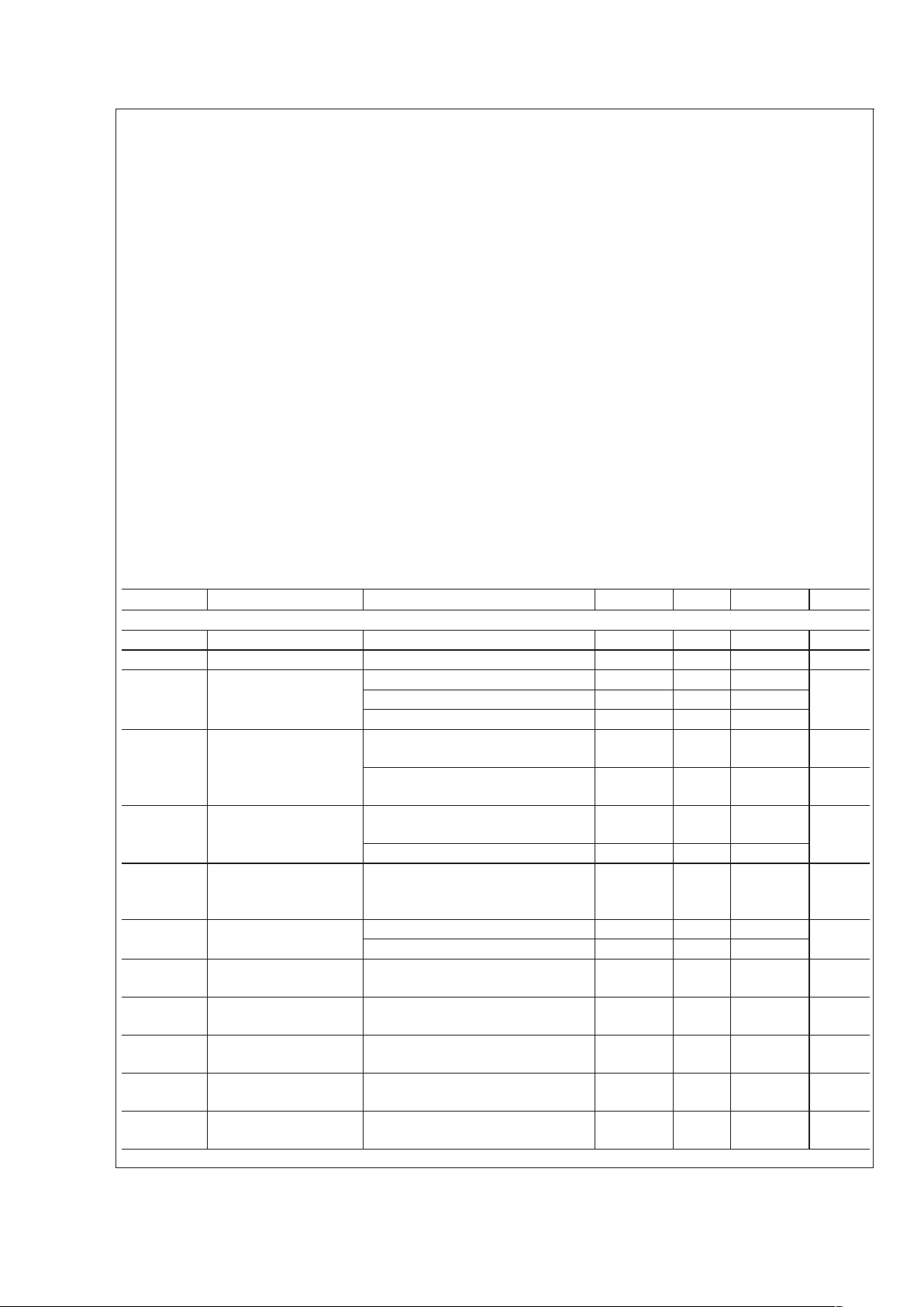
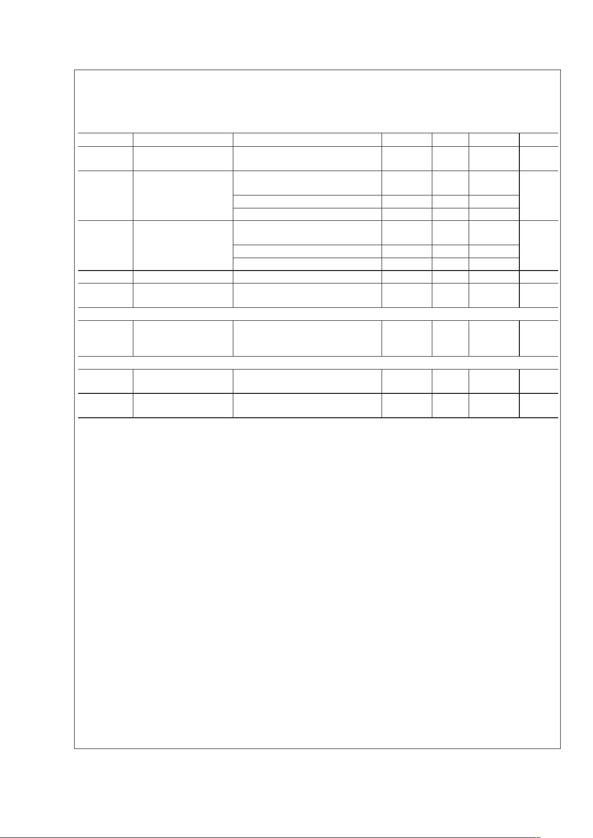
Electrical Characteristics
Unless otherwise specified, VIN= 15V, GND = PGND = 0V, VLIN5 = VDD1 = VDD2. Limits appearing in boldface type apply
over the specified operating junction temperature range, (-20˚C to +125˚C, if not otherwise specified). Specifications appearing
in plain type are measured using low duty cycle pulse testing with T
A
= 25˚C (Note 6), (Note 7). Min/Max limits are guaranteed
by design, test, or statistical analysis.
Symbol Parameter Conditions Min Typ Max Units
System
∆V
OUT/VOUT
Load Regulation VIN = 15V, V
compx
= 0.5V to 1.5V 0.04 %
∆V
OUT/VOUT
Line Regulation 5.5V ≤ VIN ≤ 30V, V
compx
=1.25V 0.04 %
V
FB1_FI2
Feedback Voltage 5.5V ≤ VIN ≤ 30V 1.215 1.238 1.260
V0˚C to 125˚C 1.217 1.259
-40˚C to 125˚C 1.212 1.261
I
VIN
Input Supply Current V
ON_SSx
>
2V
5.5V ≤ VIN ≤ 30V
1.0
2.0
mA
Shutdown (Note 8)
V
ON_SS1
=V
ON_SS2
=0V
37
110
µA
VLIN5 VLIN5 Output Voltage IVLIN5 = 0 to 25mA,
5.5V ≤ VIN ≤ 30V
4.70 5 5.30
V
-40˚C to 125˚C 4.68 5.30
V
CLos
Current Limit
Comparator Offset
(VILIMX −VRSNSX)
±
2
±
7.0 mV
I
CL
Current Limit Sink
Current
9 10 11
µA
-40˚C to 125˚C 8.67 11
I
ss_SC1
,
I
ss_SC2
Soft-Start Source
Current
V
ON_ss1
=V
ON_ss2
= 1.5V (on)
0.5 2 5.0 µA
I
ss_SK1
,
I
ss_SK2
Soft-Start Sink Current V
ON_ss1
=V
ON_ss2
=2V
2 5.2 10 µA
V
ON_SS1
,
V
ON_SS2
Soft-Start On Threshold
0.7 1.12 1.4 V
V
SSTO
Soft-Start Timeout
Threshold
(Note 9)
3.3 V
I
sc_uvdelay
UV_DELAY Source
Current
UV-DELAY = 2V
2 5 9 µA
LM2642
www.national.com 4
Electrical Characteristics (Continued)
Unless otherwise specified, VIN= 15V, GND = PGND = 0V, VLIN5 = VDD1 = VDD2. Limits appearing in boldface type apply
over the specified operating junction temperature range, (-20˚C to +125˚C, if not otherwise specified). Specifications appearing
in plain type are measured using low duty cycle pulse testing with T
A
= 25˚C (Note 6), (Note 7). Min/Max limits are guaranteed
by design, test, or statistical analysis.
Symbol Parameter Conditions Min Typ Max Units
I
sk_uvdelay
UV_DELAY Sink Current UV-DELAY = 0.4V 0.2 0.48 1.2 mA
V
UVDelay
UV_DELAY Threshold
Voltage
2.3 V
V
UVP
FB1, FB2, Under
Voltage Protection Latch
Threshold
As a percentage of nominal output
voltage (falling edge) 75 80 86 %
Hysteresis 4%
V
OVP
V
OUT
Overvoltage
Shutdown Latch
Threshold
As a percentage measured at V
FB1
,
V
FB2
107 113 122 %
V
pwrbad
Regulator Window
Detector Thresholds
(PGOOD1 from High to
Low)
As a percentage of output voltage
86.5 90.3 94.5 %
V
pwrgd
Regulator Window
Detector Thresholds
(PGOOD1 from Low to
High)
91.5 94 97.0 %
S
wx_R
SW1, SW2
ON-Resistance
V
SW1=VSW2
=2V
420 480 535 Ω
Gate Drive
I
CBOOT
CBOOTx Leakage
Current
V
CBOOT1
=V
CBOOT2
=7V
10 nA
I
SC_DRV
HDRVx and LDRVx
Source Current
V
CBOOT1
=V
CBOOT2
= 5V, VSWx=0V,
HDRVx=LDRVx=2.5V
0.5 A
I
sk_HDRV
HDRVx Sink Current V
CBOOTx
= VDDx = 5V, V
SWx
= 0V,
HDRVX = 2.5V
0.8 A
I
sk_LDRV
LDRVx Sink Current V
CBOOTx
= VDDx = 5V, V
SWx
= 0V,
LDRVX = 2.5V
1.1 A
R
HDRV
HDRV1 & 2 Source
On-Resistance
V
CBOOT1
=V
CBOOT2
= 5V,
V
SW1=VSW2
=0V
3.1 Ω
HDRV1 & 2 Sink
On-Resistance
1.5 Ω
R
LDRV
LDRV1 & 2 Source
On-Resistance
V
CBOOT1
=V
CBOOT2
= 5V,
V
SW1=VSW2
=0V
V
DD1=VDD1
=5V
3.1 Ω
LDRV1 & 2 Sink
On-Resistance
1.1 Ω
Oscillator
F
osc
Oscillator Frequency 260 300 340
kHz
-40˚C to 125˚C 257.5 340
Don_max Maximum On-Duty Cycle V
FB1=VFB2
= 1V, Measured at pins
HDRV1 and HDRV2
96 98
%
-40˚C to 125˚C 95.64
T
on_min
Minimum On-Time 166 ns
SS
OT_delta
HDRV1 and HDRV2
Delta On Time
ON/SS1 = ON/SS2 = 2V
20 150 ns
Error Amplifier
LM2642
www.national.com5
Electrical Characteristics (Continued)
Unless otherwise specified, VIN= 15V, GND = PGND = 0V, VLIN5 = VDD1 = VDD2. Limits appearing in boldface type apply
over the specified operating junction temperature range, (-20˚C to +125˚C, if not otherwise specified). Specifications appearing
in plain type are measured using low duty cycle pulse testing with T
A
= 25˚C (Note 6), (Note 7). Min/Max limits are guaranteed
by design, test, or statistical analysis.
Symbol Parameter Conditions Min Typ Max Units
I
FB1,IFB2
Feedback Input Bias
Current
V
FB1_FIX
= 1.5V, V
FB2_FIX
= 1.5V
65
±
200 nA
I
comp1_SC
,
I
comp2_SC
COMP Output Source
Current
V
FB1_FIX
=V
FB2_FIX
= 1V,
V
COMP1
=V
COMP2
=1V
18 113
µA
0˚C to 125˚C 32
-40˚C to 125˚C 6
I
comp1_SK
,
I
comp2_SK
COMP Output Sink
Current
V
FB1_FIX
=V
FB2_FIX
= 1.5V and
V
COMP1
=V
COMP2
= 0.5V
18 108
µA
0˚C to 125˚C 32
-40˚C to 125˚C 6
gm1, gm2 Transconductance 650 µmho
GI
SNS1
,
GI
SNS2
Current Sense Amplifier
(1&2) Gain
V
COMPx
= 1.25V
4.2 5.2 7.5
Voltage References and Linear Voltage Regulators
UVLO VLIN5 Under-voltage
Lockout
Threshold Rising
ON/SS1, ON/SS2 transition
from low to high 3.6 4.0 4.4 V
Logic Outputs
I
OL
PGOOD Low Sink
Current
V
PGOOD
= 0.4V
0.60 0.95 mA
I
OH
PGOOD High Leakage
Current
V
PGOOD
=5V
5 200 nA
Note 1: Absolute maximum ratings indicate limits beyond which damage to the device may occur. Operating Range indicates conditions for which the device is
intended to be functional, but does not guarantee specfic performance limits. For guaranteed specifications and test conditions, see the Electrical Characteristics.
The guaranteed specifications apply only for the test conditions. Some performance characteristics may degrade when the device is not operated under the listed
test conditions.
Note 2: ON/SS1 and ON/SS2 are internally pulled up to one diode drop above VLIN5. Do not apply an external pull-up voltage to these pins. It may cause damage
to the IC.
Note 3: The maximum allowable power dissipation is calculated by using P
DMAX
=(T
JMAX-TA
)/θJA, where T
JMAX
is the maximum junction temperature, TAis the
ambient temperature and θ
JA
is the junction-to-ambient thermal resistance of the specified package. The 1.1W rating results from using 125˚C, 25˚C, and 90.6˚C/W
for T
JMAX,TA
, and θJArespectively. A θJAof 90.6˚C/W represents the worst-case condition of no heat sinking of the 28-pin TSSOP. A thermal shutdown will occur
if the temperature exceeds the maximum junction temperature of the device.
Note 4: For detailed information on soldering plastic small-outline packages, refer to the Packaging Databook available from National Semiconductor Corporation.
Note 5: For testing purposes, ESD was applied using the human-body model, a 100pF capacitor discharged through a 1.5kΩ resistor.
Note 6: A typical is the center of characterization data measured with low duty cycle pulse tsting at T
A
= 25˚C. Typicals are not guaranteed.
Note 7: All limits are guaranteed. All electrical characteristics having room-temperature limits are tested during production with T
A=TJ
= 25˚C. All hot and cold limits
are guaranteed by correlating the electrical characteristics to process and temperature variations and applying statistical process control.
Note 8: Both switching controllers are off. The linear regulator VLIN5 remains on.
Note 9: When SS1 and SS2 pins are charged above this voltage and either of the output voltages at Vout1 or Vout2 is still below the regulation limit, the under
voltage protection feature is initialized.
LM2642
www.national.com 6

20046203
FIGURE 1. Typical 2 Channel Application Circuit
LM2642
www.national.com7

20046204
FIGURE 2. Typical Single Channel Application Circuit
LM2642
www.national.com 8

Block Diagram
20046205
LM2642
www.national.com9

Typical Performance Characteristics
Softstart Waveforms
(I
LOAD1=ILOAD2
= 0A)
Power On and PGOOD1 Waveforms
(I
LOAD1=ILOAD2
= 0A)
20046223 20046221
UVP Startup Waveforms
Over-Current and UVP Shutdown
(I
LOAD2
= 0A)
20046268 20046220
Shutdown Waveforms
(I
LOAD1=ILOAD2
= 0A)
Ch.1 Load Transient Response
5V
OUT
, 12V
IN
20046222
20046265
LM2642
www.national.com 10

Typical Performance Characteristics (Continued)
Ch.2 Load Transient Response
3.3V
OUT
, 12V
IN
Load Transient Response
Parallel Operation 1.8V
OUT
, 12V
IN
20046229 20046228
Input Supply Current vs Temperature
(Shutdown Mode V
IN
= 15V)
Input Supply Current vs V
IN
Shutdown Mode (25˚C)
20046224
20046225
VLIN5 vs Temperature VLIN5 vs VIN(25˚C)
20046226 20046227
LM2642
www.national.com11

Typical Performance Characteristics (Continued)
FB Reference Voltage vs Temperature Operating Frequency vs Temperature
20046266
20046267
Error Amplifier Gain vs Temperature
Efficiency vs Load Current
Ch.1 = 5V, Ch.2 = Off
20046269
20046270
Efficiency vs Load Current
Ch.2 = 2.5V, Ch.1 = Off
Efficiency vs Load Current
Ch.2 = 3.3V, Ch.1 = Off
20046271
20046272
LM2642
www.national.com 12

Operation Descriptions
SOFT START
The ON/SS1 pin has dual functionality as both channel
enable and soft start control. The soft start block diagram is
shown in Figure 3.
The LM2642 will remain in shutdown mode while both soft
start pins are grounded.In a normal application (with a soft
start capacitor connected between the ON/SS1 pin and
SGND) soft start functions as follows. As the input voltage
rises (note: Iss starts to flow when VIN ≥ 2.2V), the internal
5V LDO starts up, and an internal 2µA current charges the
soft start capacitor. During soft start phase, the error amplifier output voltage at the COMPx pin is clamped at 0.55V
and the duty cycle is controlled only by the soft start voltage.
As the SSx pin voltage ramps up, the duty cycle increases
proportional to the soft start ramp, causing the output voltage
to ramp up. The rate at which the duty cycle increases
depends on the capacitance of the soft start capacitor. The
higher the capacitance, the slower the output voltage ramps
up. When the corresponding output voltage exceeds 98%
(typical) of the set target voltage, the regulator switches from
soft start to normal operating mode. At this time, the 0.55V
clamp at the output of the error amplifier releases and peak
current feedback control takes over. Once in peak current
feedback control mode, the output of the error amplifier will
travel within the 0.5V and 2V window to achieve PWM
control. See Figure 4.
During soft start, over-voltage protection and current limit
remain in effect. The under voltage protection feature is
activated when the ON/SS pin exceeds the timeout threshold (3.3V typical). If the ON/SSx capacitor is too small, the
duty cycle may increase too rapidly, causing the device to
latch off due to output voltage overshoot above the OVP
threshold. This becomes more likely in applications requiring
low output voltage, high input voltage and light load. A
capacitance of 10nF is recommended at each soft start pin
to provide a smooth monotonic output ramp.
SEQUENTIAL STARTUP
Sequential startup can be implemented by simply connecting
PGOOD1 to SS/ON2. Once channel 1 has reached 94% of
nominal, PGOOD1 will go high, thus enabling SS/ON2. In
this mode of operation, channel 2 will be controlled by the
state of channel 1. If channel 1 falls out of the PGOOD1
window, channel 2 will be switched off immediately.
OVER VOLTAGE PROTECTION (OVP)
If the output voltage on either channel rises above 113% of
nominal, over voltage protection activates. Both channels
will latch off, and the PGOOD1 pin will go low. When the
OVP latch is set, the high side FET driver, HDRVx, is immediately turned off and the low side FET driver, LDRVx, is
turned on to discharge the output capacitor through the
inductor. To reset the OVP latch, either the input voltage
must be cycled, or both channels must be switched off.
UNDER VOLTAGE PROTECTION (UVP) AND UV DELAY
If the output voltage on either channel falls below 80% of
nominal, under voltage protection activates. As shown in
Figure 5, an under-voltage event will shut off the UV_DELAY
MOSFET, which will allow the UV_DELAY capacitor to
charge at 5uA (typical). At the UV_DELAY threshold (2.3V
20046206
FIGURE 3. Soft Start and ON/OFF
20046207
FIGURE 4. Voltage Clamp at COMPx Pin
20046208
FIGURE 5. PGOOD, OVP and UVP
LM2642
www.national.com13

Operation Descriptions (Continued)
typical) both channels will latch off. Also, UV_DELAY will be
disabled and the UV_DELAY pin will return to 0V. During
UVP, both the high side and low side FET drivers will be
turned off. If no capacitor is connected to the UV_DELAY pin,
the UVP latch will be activated immediately. To reset the
UVP latch, either the input voltage must be cycled, or both
ON/SS pins must be pulled low. The UVP function can be
disabled by connecting the UV_DELAY pin to ground.
POWER GOOD
A power good pin (PGOOD1) is available to monitor the
output status of Channel 1. As shown in Figure 5, the pin
connects to the output of an open drain MOSFET, which will
remain open while Channel 1 is within operating range.
PGOOD1 will go low (low impedance to ground) under the
following four conditions:
1. Channel 1 is turned off
2. Channel 1 output falls below 90.3% of nominal (UVPG1)
3. OVP on either channel
4. UVP on either channel
When on, the PGOOD1 pin is capable of sinking 0.95mA
(typical). If an OVP or UVP condition occurs, both channels
will latch off, and the PGOOD1 pin will be latched low. During
a UVPG1 condition, however, PGOOD1 will not latch off. The
pin will stay low until Channel 1 output voltage returns to
94% (typical) of nominal. See Vpwrgd in the Electrical Characteristics table.
OUTPUT CAPACITOR DISCHARGE
Each channel has an embedded 480Ω MOSFET with the
drain connected to the SWx pin. This MOSFET will discharge the output capacitor of its channel if its channel is off,
or the IC enters a fault state caused by one of the following
conditions:
1. UVP
2. UVLO
3. Thermal shut-down (TSD)
If an output over voltage event occurs, the HDRVx will be
turned off and LDRVx will be turned on immediately to
discharge the output capacitor of both channels through the
inductor.
SWITCHING NOISE REDUCTION
Power MOSFETs are very fast switching devices. In synchronous rectifier converters, the rapid increase of drain
current in the top FET coupled with parasitic inductance will
generate unwanted Ldi/dt noise spikes at the source node of
the FET (SWx node) and also at the VIN node. The magnitude of this noise will increase as the output current increases. This parasitic spike noise may turn into electromagnetic interference (EMI), and can also cause problems in
device performance. Therefore, it must be suppressed using
one of the following methods.
It is strongly recommended to add R-C filters to the current
sense amplifier inputs as shown in Figure 7. This will reduce
the susceptibility to switching noise, especially during heavy
load transients and short on time conditions. The filter components should be connected as close as possible to the IC.
As shown in Figure 6, adding a resistor in series with the
SWx pin will slow down the gate drive (HDRVx), thus slowing
the rise and fall time of the top FET, yielding a longer drain
current transition time.
Usually a 3.3Ω to 4.7Ω resistor is sufficient to suppress the
noise. Top FET switching losses will increase with higher
resistance values.
Small resistors (1-5 ohms) can also be placed in series with
the HDRVx pin or the CBOOTx pin to effectively reduce
switch node ringing. A CBOOT resistor will slow the rise time
of the FET, whereas a resistor at HDRV will reduce both rise
and fall times.
CURRENT SENSING AND LIMITING
As shown in Figure 7, the KSx and RSNSx pins are the
inputs of the current sense amplifier. Current sensing is
accomplished either by sensing the Vds of the top FET or by
sensing the voltage across a current sense resistor connected from VIN to the drain of the top FET. The advantage
of sensing current across the top FET are reduced parts
count, cost and power loss, whereas using a current sense
resistor improves the current sense accuracy. Keeping the
differential current-sense voltage below 200mV ensures linear operation of the current sense amplifier. Therefore, the
Rdson of the top FET or the current sense resistor must be
small enough so that the current sense voltage does not
exceed 200mV when the top FET is on. There is a leading
edge blanking circuit that forces the top FET on for at least
166ns. Beyond this minimum on time, the output of the PWM
comparator is used to turn off the top FET. Additionally, a
minimum voltage of at least 50mV across Rsns is recommended to ensure a high SNR at the current sense amplifier.
Assuming a maximum of 200mV across Rsns, the current
sense resistor can be calculated as follows:
where Imax is the maximum expected load current, including
overload multiplier (ie:120%), and Irip is the inductor ripple
current (See equation 7). The above equation gives the
maximum allowable value for Rsns. Switching losses will
increase with Rsns, thus lowering efficiency.
The peak current limit is set by an external resistor connected between the ILIMx pin and the KSx pin. An internal
10µA current sink on the ILIMx pin produces a voltage
across the resistor to set the current limit threshold which is
compared to the current sense voltage. A 10nF capacitor
across this resistor is required to filter unwanted noise that
could improperly trip the current limit comparator.
20046209
FIGURE 6. SW Series Resistor
LM2642
www.national.com 14

Operation Descriptions (Continued)
Current limit is activated when the inductor current is high
enough to cause the voltage at the RSNSx pin to be lower
than that of the ILIMx pin. This toggles the comparator, thus
turning off the top FET immediately. The comparator is disabled either when the top FET is turned off or during the
leading edge blanking time. The equation for current limit
resistor, R
lim
, is as follows:
Where Ilim is the load current at which the current limit
comparator will be tripped.
When sensing current across the top FET, replace Rsns with
the Rdson of the FET. This calculated Rlim value guarantees
that the minimum current limit will not be less than Imax. It is
recommended that a 1% tolerance resistor be used.
When sensing across the top FET, Rdson will show more
variation than a current sense resistor, largely due to temperature. Rdson will increase proportional to temperature
according to a specific temperature coefficient. Refer to the
manufacturer’s datasheet to determine the range of Rdson
values over operating temperature or see the Component
Selection section (equation 12) for a calculation of maximum
Rdson. This will prevent Rdson variations from prematurely
setting off the current limit comparator as the operating
temperature increases.
To ensure accurate current sensing, special attention in
board layout is required. The KSx and RSNSx pins require
separate traces to form a Kelvin connection to the corresponding current sense nodes.
INPUT UNDER VOLTAGE LOCKOUT (UVLO)
The input under-voltage lock out threshold, which is sensed
via the VLIN5 internal LDO output, is 4.0V (typical). Below
this threshold, both HDRVx and LDRVx will be turned off and
the internal 480Ω MOSFETs will be turned on to discharge
the output capacitors through the SWx pins. During UVLO,
the ON/SS pins will sink 5mA to discharge the soft start
capacitors and turn off both channels. As the input voltage
increases again above 4.0V, UVLO will be de-activated, and
the device will restart again from soft start phase. If the
voltage at VLIN5 remains below 4.5V, but above the 4.0V
UVLO threshold, the device cannot be guaranteed to operate within specification.
If the input voltage is between 4.0V and 5.2V, the VLIN5 pin
will not regulate, but will follow approximately 200mV below
the input voltage.
DUAL-PHASE PARALLEL OPERATION
In applications with high output current demand, the two
switching channels can be configured to operate as a two180˚ out of phase converter to provide a single output voltage with current sharing between the two switching channels. This approach greatly reduces the stress and heat on
the output stage components while lowering input ripple
current. The sum of inductor ripple current is also reduced
which results in lowering output ripple voltage. Figure 2
shows an example of a typical two-phase circuit. Because
precision current sense is the primary design criteria to
ensure accurate current sharing between the two channels,
both channels must use external sense resistors for current
sensing. To minimize the error between the error amplifiers
of the two channels, tie the feedback pins FB1 and FB2
together and connect to a single voltage divider for output
voltage sensing. Also, tie the COMP1 and COMP2 together
and connect to the compensation network. ON/SS1 and
ON/SS2 must be tied together to enable and disable both
channels simultaneously.
Component Selection
OUTPUT VOLTAGE SETTING
The output voltage for each channel is set by the ratio of a
voltage divider as shown in Figure 8. The resistor values can
be determined by the following equation:
(1)
Where Vfb=1.238V. Although increasing the value of R1 and
R2 will increase efficiency, this will also decrease accuracy.
Therefore, a maximum value is recommended for R2 in
order to keep the output within .3% of Vnom. This maximum
R2 value should be calculated first with the following equation:
(2)
Where 200nA is the maximum current drawn by FBx pin.
Example: Vnom=5V, Vfb=1.238V, Ifbmax=200nA.
20046210
FIGURE 7. Current Sense and Current Limit
20046211
FIGURE 8. Output Voltage Setting
LM2642
www.national.com15

Component Selection (Continued)
(3)
Choose 60K
(4)
The output voltage is limited by the maximum duty cycle as
well as the minimum on time. Figure 9 shows the limits for
input and output voltages. The recommended maximum output voltage is approximately 1V less than the nominal input
voltage. At 30V input, the minimum output is approximately
2.3V and the maximum is approximately 27V.
For input voltages below 5.5V, VLIN5 must be connected to
Vin through a small resistor (approximately 4.7 ohm). This
will ensure that VLIN5 does not fall below the UVLO threshold.
Output Capacitor Selection
In applications that exhibit large and fast load current
swings, the slew rate of such a load current transient may be
beyond the response speed of the regulator. Therefore, to
meet voltage transient requirements during worst-case load
transients, special consideration should be given to output
capacitor selection. The total combined ESR of the output
capacitors must be lower than a certain value, while the total
capacitance must be greater than a certain value. Also, in
applications where the specification of output voltage regulation is tight and ripple voltage must be low, starting from the
required output voltage ripple will often result in fewer design
iterations.
ALLOWED TRANSIENT VOLTAGE EXCURSION
The allowed output voltage excursion during a load transient
(∆Vc_s) is:
Where±δ% is the output voltage regulation window and
±
e% is the output voltage initial accuracy.
Example: Vnom = 5V, δ% = 7%, e% = 3.4%, Vrip = 40mV
peak to peak.
Since the ripple voltage is included in the calculation of
∆Vc_s, the inductor ripple current should not be included in
the worst-case load current excursion. That is, the worstcase load current excursion should be simply maximum load
current change specification, ∆Ic_s.
MAXIMUM ESR CALCULATION
Unless the rise and fall times of a load transient are slower
than the response speed of the control loop, if the total
combined ESR (Re) is too high, the load transient requirement will not be met, no matter how large the capacitance.
The maximum allowed total combined ESR is:
Example: ∆Vc_s = 160mV, ∆Ic_s = 3A. Then Re_max =
53.3mΩ.
Maximum ESR criterion can be used when the associated
capacitance is high enough, otherwise more capacitors than
the number determined by this criterion should be used in
parallel.
MINIMUM CAPACITANCE CALCULATION
In a switch mode power supply, the minimum output capacitance is typically dictated by the load transient requirement.
If there is not enough capacitance, the output voltage excursion will exceed the maximum allowed value even if the
maximum ESR requirement is met. The worst-case load
transient is an unloading transient that happens when the
input voltage is the highest and when the present switching
cycle has just finished. The corresponding minimum capacitance is calculated as follows:
Notice it is already assumed the total ESR, Re, is no greater
than Re_max, otherwise the term under the square root will
be a negative value. Also, it is assumed that L has already
been selected, therefore the minimum L value should be
calculated before Cmin and after Re (see Inductor Selection
below). Example: Re = 20mΩ,Vnom=5V,∆Vc_s = 160mV,
∆Ic_s = 3A, L = 8µH
Generally speaking, Cmin decreases with decreasing Re,
∆Ic_s, and L, but with increasing Vnom and ∆Vc_s.
20046213
FIGURE 9. Available Output Voltage Range
LM2642
www.national.com 16

Inductor Selection
The size of the output inductor can be determined from the
desired output ripple voltage, Vrip, and the impedance of the
output capacitors at the switching frequency. The equation to
determine the minimum inductance value is as follows:
In the above equation, Re is used in place of the impedance
of the output capacitors. This is because in most cases, the
impedance of the output capacitors at the switching frequency is very close to Re. In the case of ceramic capacitors, replace Re with the true impedance.
Example: Vin (max)= 30V, Vnom = 5.0V, Vrip = 40mV, Re
=20mΩ, f = 300kHz
Lmin = 7µH
The actual selection process usually involves several itera-
tions of all of the above steps, from ripple voltage selection,
to capacitor selection, to inductance calculations. Both the
highest and the lowest input and output voltages and load
transient requirements should be considered. If an inductance value larger than Lmin is selected, make sure that the
Cmin requirement is not violated.
Priority should be given to parameters that are not flexible or
more costly. For example, if there are very few types of
capacitors to choose from, it may be a good idea to adjust
the inductance value so that a requirement of 3.2 capacitors
can be reduced to 3 capacitors.
Since inductor ripple current is often the criterion for selecting an output inductor, it is a good idea to double-check this
value. The equation is:
Where D is the duty cycle, defined by V
nom/Vin
.
Also important is the ripple content, which is defined by Irip
/Inom. Generally speaking, a ripple content of less than 50%
is ok. Larger ripple content will cause too much loss in the
inductor.
Example: Vin = 12V, Vnom = 5.0V, f = 300kHz, L = 8µH
Given a maximum load current of 3A, the ripple content is
1.2A / 3A = 40%.
When choosing the inductor, the saturation current should
be higher than the maximum peak inductor current and the
RMS current rating should be higher than the maximum load
current.
Input Capacitor Selection
The fact that the two switching channels of the LM2642 are
180˚ out of phase will reduce the RMS value of the ripple
current seen by the input capacitors. This will help extend
input capacitor life span and result in a more efficient system. Input capacitors must be selected that can handle both
the maximum ripple RMS current at highest ambient temperature as well as the maximum input voltage. In applications in which output voltages are less than half of the input
voltage, the corresponding duty cycles will be less than 50%.
This means there will be no overlap between the two channels’ input current pulses. The equation for calculating the
maximum total input ripple RMS current for duty cycles
under 50% is:
where I1 is maximum load current of Channel 1, I2 is the
maximum load current of Channel 2, D1 is the duty cycle of
Channel 1, and D2 is the duty cycle of Channel 2.
Example: Imax_1 = 3.6A, Imax_2 = 3.6A, D1 = 0.42, and D2
= 0.275
Choose input capacitors that can handle 1.66A ripple RMS
current at highest ambient temperature. In applications
where output voltages are greater than half the input voltage,
the corresponding duty cycles will be greater than 50%, and
there will be overlapping input current pulses. Input ripple
current will be highest under these circumstances. The input
RMS current in this case is given by:
Where, again, I1 and I2 are the maximum load currents of
channel 1 and 2, and D1 and D2 are the duty cycles. This
equation should be used when both duty cycles are expected to be higher than 50%.
Input capacitors must meet the minimum requirements of
voltage and ripple current capacity. The size of the capacitor
should then be selected based on hold up time requirements. Bench testing for individual applications is still the
best way to determine a reliable input capacitor value. The
input capacitor should always be placed as close as possible
to the current sense resistor or the drain of the top FET.
MOSFET Selection
BOTTOM FET SELECTION
During normal operation, the bottom FET is switching on and
off at almost zero voltage. Therefore, only conduction losses
are present in the bottom FET. The most important parameter when selecting the bottom FET is the on resistance
(Rdson). The lower the on resistance, the lower the power
loss. The bottom FET power loss peaks at maximum input
voltage and load current. The equation for the maximum
allowed on resistance at room temperature for a given FET
package, is:
LM2642
www.national.com17

MOSFET Selection (Continued)
where Tj_max is the maximum allowed junction temperature
in the FET, Ta_max is the maximum ambient temperature,
R
θja
is the junction-to-ambient thermal resistance of the FET,
and TC is the temperature coefficient of the on resistance
which is typically in the range of 10,000ppm/˚C.
If the calculated Rdson_max is smaller than the lowest value
available, multiple FETs can be used in parallel. This effectively reduces the Imax term in the above equation, thus
reducing Rdson. When using two FETs in parallel, multiply
the calculated Rdson_max by 4 to obtain the Rdson_max for
each FET. In the case of three FETs, multiply by 9.
If the selected FET has an Rds value higher than 35.3Ω,
then two FETs with an Rdson less than 141mΩ (4 x 35.3mΩ)
can be used in parallel. In this case, the temperature rise on
each FET will not go to Tj_max because each FET is now
dissipating only half of the total power.
TOP FET SELECTION
The top FET has two types of losses: switching loss and
conduction loss. The switching losses mainly consist of
crossover loss and bottom diode reverse recovery loss.
Since it is rather difficult to estimate the switching loss, a
general starting point is to allot 60% of the top FET thermal
capacity to switching losses. The best way to precisely determine switching losses is through bench testing. The equation for calculating the on resistance of the top FET is thus:
Example: Tj_max = 100˚C, Ta_max = 60˚C, Rqja = 60˚C/W,
Vin_min = 5.5V, Vnom = 5V, and Iload_max = 3.6A.
When using FETs in parallel, the same guidelines apply to
the top FET as apply to the bottom FET.
Loop Compensation
The general purpose of loop compensation is to meet static
and dynamic performance requirements while maintaining
stability. Loop gain is what is usually checked to determine
small-signal performance. Loop gain is equal to the product
of control-output transfer function and the output-control
transfer function (the compensation network transfer function). Generally speaking it is a good idea to have a loop gain
slope that is -20dB /decade from a very low frequency to well
beyond the crossover frequency. The crossover frequency
should not exceed one-fifth of the switching frequency, i.e.
60kHz in the case of LM2642. The higher the bandwidth is,
the faster the load transient response speed will potentially
be. However, if the duty cycle saturates during a load transient, further increasing the small signal bandwidth will not
help. Since the control-output transfer function usually has
very limited low frequency gain, it is a good idea to place a
pole in the compensation at zero frequency, so that the low
frequency gain will be relatively large. A large DC gain
means high DC regulation accuracy (i.e. DC voltage
changes little with load or line variations). The rest of the
compensation scheme depends highly on the shape of the
control-output plot.
As shown in Figure 10, the control-output transfer function
consists of one pole (fp), one zero (fz), and a double pole at
fn (half the switching frequency). The following can be done
to create a -20dB /decade roll-off of the loop gain: Place the
first pole at 0Hz, the first zero at fp, the second pole at fz,
and the second zero at fn. The resulting output-control transfer function is shown in Figure 11.
20046214
FIGURE 10. Control-Output Transfer Function
LM2642
www.national.com 18

Loop Compensation (Continued)
The control-output corner frequencies, and thus the desired
compensation corner frequencies, can be determined approximately by the following equations:
Since fp is determined by the output network, it will shift with
loading (Ro) and duty cycle. First determine the range of
frequencies (fpmin/max) of the pole across the expected
load range, then place the first compensation zero within that
range.
Example: R
e
= 20mΩ,Co= 100µF, R
omax
= 5V/100mA =
50Ω,R
omin
= 5V/3A = 1.7Ω:
Once the fp range is determined, Rc1should be calculated
using:
Where B is the desired gain in V/V at fp (fz1), gm is the
transconductance of the error amplifier, and R1 and R2 are
the feedback resistors. A gain value around 10dB (3.3v/v) is
generally a good starting point.
Example: B = 3.3 v/v, gm=650 m, R1 = 20 KΩ, R2 = 60.4 KΩ:
Bandwidth will vary proportional to the value of Rc1. Next,
Cc1 can be determined with the following equation:
Example: fpmin = 363 Hz, Rc1=20 KΩ:
The value of Cc1should be within the range determined by
Fpmin/max. A higher value will generally provide a more
stable loop, but too high a value will slow the transient
response time.
The compensation network (Figure 12) will also introduce a
low frequency pole which will be close to 0Hz.
A second pole should also be placed at fz. This pole can be
created with a single capacitor Cc2 and a shorted Rc2 (see
Figure 12). The minimum value for this capacitor can be
calculated by:
Cc2 may not be necessary, however it does create a more
stable control loop. This is especially important with high
load currents and in current sharing mode.
Example: fz = 80 kHz, Rc1 = 20 KΩ:
A second zero can also be added with a resistor in series
with Cc2. If used, this zero should be placed at fn, where the
control to output gain rolls off at -40dB/dec. Generally, fn will
be well below the 0dB level and thus will have little effect on
stability. Rc2 can be calculated with the following equation:
20046212
FIGURE 11. Output-Control Transfer Function
20046274
FIGURE 12. Compensation Network
LM2642
www.national.com19

Physical Dimensions inches (millimeters)
unless otherwise noted
28-Lead TSSOP Package
Order Number LM2642MTC
NS Package Number MTC28
LIFE SUPPORT POLICY
NATIONAL’S PRODUCTS ARE NOT AUTHORIZED FOR USE AS CRITICAL COMPONENTS IN LIFE SUPPORT
DEVICES OR SYSTEMS WITHOUT THE EXPRESS WRITTEN APPROVAL OF THE PRESIDENT AND GENERAL
COUNSEL OF NATIONAL SEMICONDUCTOR CORPORATION. As used herein:
1. Life support devices or systems are devices or
systems which, (a) are intended for surgical implant
into the body, or (b) support or sustain life, and
whose failure to perform when properly used in
accordance with instructions for use provided in the
labeling, can be reasonably expected to result in a
significant injury to the user.
2. A critical component is any component of a life
support device or system whose failure to perform
can be reasonably expected to cause the failure of
the life support device or system, or to affect its
safety or effectiveness.
National Semiconductor
Americas Customer
Support Center
Email: new.feedback@nsc.com
Tel: 1-800-272-9959
National Semiconductor
Europe Customer Support Center
Fax: +49 (0) 180-530 85 86
Email: europe.support@nsc.com
Deutsch Tel: +49 (0) 69 9508 6208
English Tel: +44 (0) 870 24 0 2171
Français Tel: +33 (0) 1 41 91 8790
National Semiconductor
Asia Pacific Customer
Support Center
Email: ap.support@nsc.com
National Semiconductor
Japan Customer Support Center
Fax: 81-3-5639-7507
Email: jpn.feedback@nsc.com
Tel: 81-3-5639-7560
www.national.com
LM2642 Two-Phase Synchronous Step-Down Switching Controller
National does not assume any responsibility for use of any circuitry described, no circuit patent licenses are implied and National reserves the right at any time without notice to change said circuitry and specifications.
 Loading...