

LM2641
Dual Adjustable Step-Down Switching Power Supply
Controller
General Description
The LM2641 is a dual step-down power supply controller intended for application in notebook personal computers and
other battery-powered equipment.
Fixed-frequency synchronous drive of logic-level N-channel
power MOSFETs is combined with an optional
pulse-skipping mode to achieve ultra efficient powerconversion over a 1000:1 load current range. The pulse-skipping
mode can be disabled in favor of fixed-frequency operation
regardless of the load current level.
High DC gain and current-mode feedback control assure excellent line and load regulation and a wide loop bandwidth
for fast response to dynamic loads.
An internal oscillator fixes the switching frequency at
300 kHz. Optionally, switching can be synchronized to an external clock running as fast as 400 kHz.
An optional soft-start feature limits current surges from the
input power supply at start up and provides a simple means
of start-up sequencing.
Logic-level inputs allow the controllers to be turned ON and
OFF separately.
Key Specifications
n 96%efficient
n 5.5 to 30V input range
n Dual outputs adjustable from 2.2 to 8V
n 0.5%typical load regulation error
n 0.002%/V typical line regulation error
Features
n 300 kHz fixed-frequency switching
n Switching synchronization with an external signal up to
400 kHz
n Optional pulse-skipping mode
n Adjustable secondary feedback
n Input undervoltage lockout
n Output undervoltage shutdown protection
n Output overvoltage shutdown protection
n Programmable soft-start (each controller)
n 5V, 50 mA linear regulator output
n Precision 2.5V reference output
n 28-pin TSSOP
Applications
n Notebook and subnotebook computers
n Wireless data terminals
n Battery-powered instruments
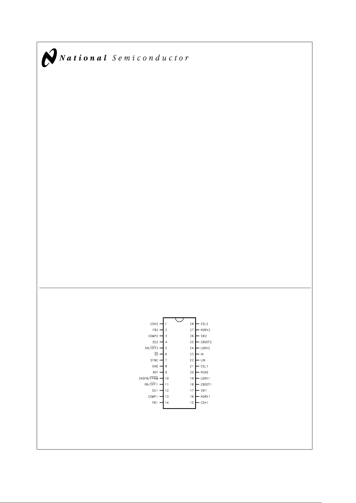
Connection Diagram and Ordering Information
28-Lead TSSOP (MTC)
DS100949-1
Top View
Order Number LM2641MTC-ADJ
See NS Package Number MTC28
January 2000
LM2641 Dual Adjustable Step-Down Switching Power Supply Controller
© 2000 National Semiconductor Corporation DS100949 www.national.com
Pin Description (Refer to Typical Application Circuits)
Pin
#
Name Function
1 CSH2 The sense point for the positive side of the voltage across the current sense resistor (R13)
placed in series with output
#
2.
2 FB2 The regulated output voltage appearing at output
#
2 is sensed using this pin by connecting it to
the center of the output resistive divider (R15 and R16).
3 COMP2 An R-C network made up of R11, C10, and C12 is connected to this pin which provides loop
compensation for regulated output
#
2.
4 SS2 This provides programmable soft-start for the
#
2 output along with capacitor C15.
5 ON/OFF2
This pin turns off only output#2.
6SD
The part can be put into “sleep” mode using this pin, where both outputs are off and the internal
chip functions are shut down.
7 SYNC The internal oscillator may be synchronized to an external clock via this pin.
8 GND Connect this pin to circuit Signal Ground.
9 REF Internal 2.5V reference voltage. This voltage is turned off by the SD pin, but remains on if either
or both ON/OFF pins are pulled low, which turns off the regulated output(s).
10 2NDFB/FPWM A 12V supply can be generated using an auxiliary winding on the 5V output inductor. Feedback
to control this 12V output is brought in through this pin. If the 12V supply is not required, this
pin can also force the chip to operate at fixed frequency at light loads by pulling the pin low
(this is the “forced-PWM” mode of operation). This will prevent the converter from operating in
pulse-skipping mode.
11 ON/OFF1
This pin turns off only output#1.
12 SS1 This provides programmable soft-start for the
#
1 output along with capacitor C3.
13 COMP1 An R-C network made up of R6, C5, and C7 is connected to this pin which provides loop
compensation for regulated output
#
1.
14 FB1 The regulated output voltage appearing at output
#
1 is sensed using this pin by connecting it to
the center of the output resistive divider (R1 and R2).
15 CSH1 The sense point for the positive side of the voltage across the current sense resistor (R4)
placed in series with output
#
1.
16 HDRV1 The drive for the gate of the high-side switching FET used for output
#
1.
17 SW1 This is the switching output drive point of the two power FETs which produce output
#
1.
18 CBOOT1 The bootstrap capacitor (C8) for output
#
1 is returned to this point.
19 LDRV1 The drive for the gate of the low-side switching FET (synchronous rectifier) used for output
#
1.
20 PGND Connect this pin to circuit Power Ground.
21 CSL1 The sense point for the negative side of the voltage across the current sense resistor (R4)
placed in series with output
#
1.
22 LIN This pin provides a low-current (50 mA max) 5V output. This output is always on, and can not
be turned off by either the SD or ON/OFF pins.
23 IN This is the connection for the main input power.
24 LDRV2 The drive for the gate of the low-side switching FET (synchronous rectifier) used for output
#
2.
25 CBOOT2 The bootstrap capacitor (C9) for output
#
2 is returned to this point.
26 SW2 This is the switching output drive point of the two power FETs which produce output
#
2.
27 HDRV2 The drive for the gate of the high-side switching FET used for output
#
2.
28 CSL2 The sense point for the negative side of the voltage across the current sense resistor (R13)
placed in series with output
#
2.
LM2641
www.national.com 2
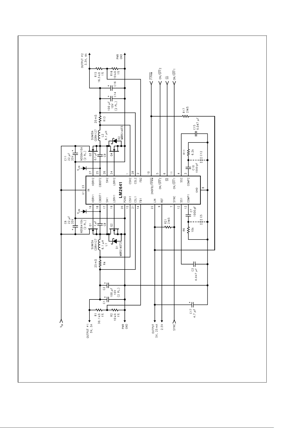
Typical Application Circuits
DS100949-3
FIGURE 1. Application With 5V/3A and 3.3V/4A Outputs
LM2641
www.national.com3
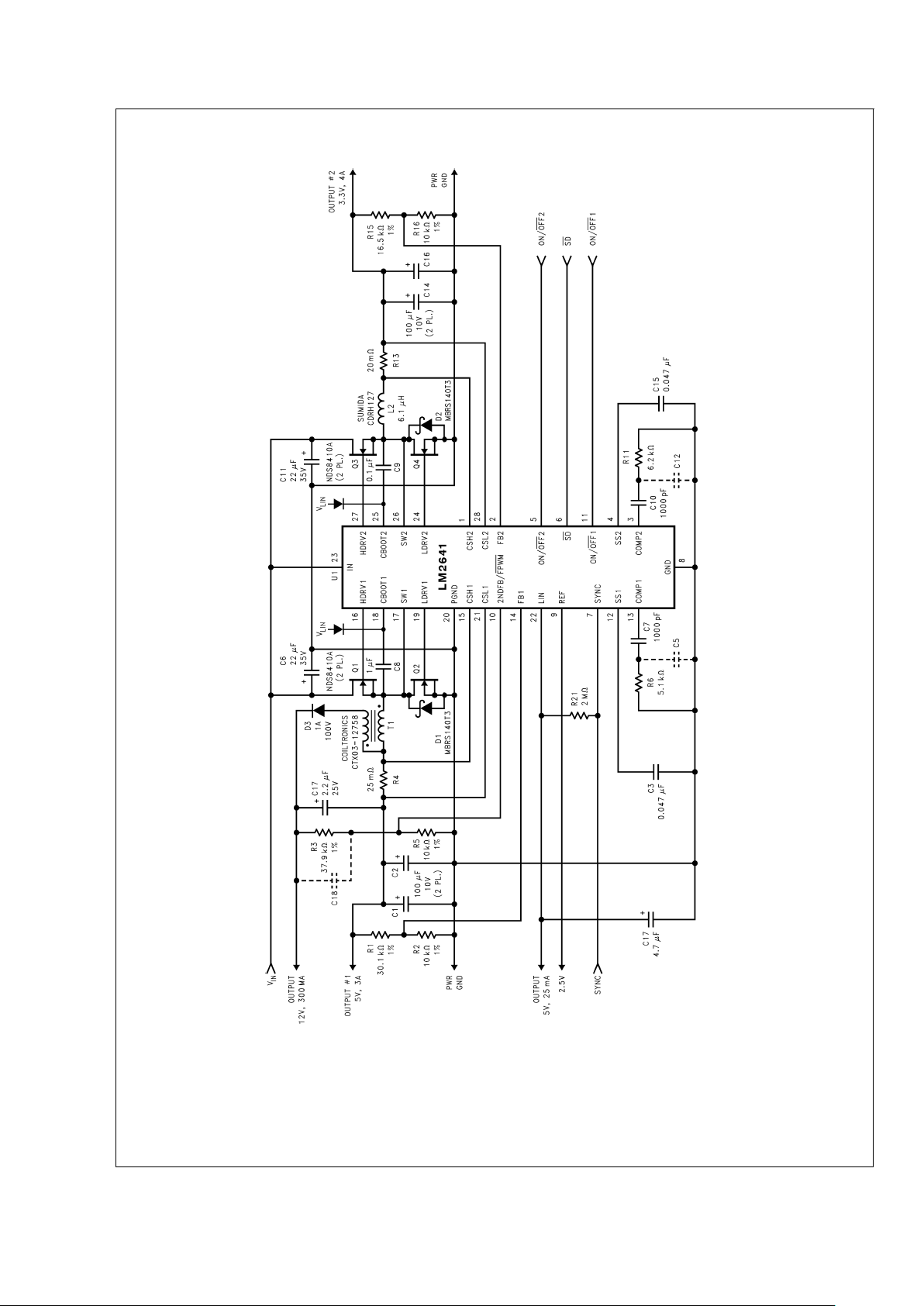
Typical Application Circuits (Continued)
DS100949-4
FIGURE 2. Application With 5V/3A, 3.3V/4A, and 12V/0.3A Outputs
LM2641
www.national.com 4
Absolute Maximum Ratings (Notes 2, 1)
If Military/Aerospace specified devices are required,
please contact the National Semiconductor Sales Office/
Distributors for availability and specifications.
IN, SW1, and SW2 −0.3 to 31V
FB1 and FB2 −0.3 to 3V
SD, ON/OFF1, ON/OFF2,
2NDFB/FPWM, SYNC, REF,
SS1, SS2, COMP1,
COMP2 and CSL1
−0.3 to (V
LIN
+0.3)V
LIN −0.3 to 6V
CSH1, CSH2, and CSL2 (Note
12)
−0.3 to 9V
Voltage from CBOOT1 to SW1
and from CBOOT2 to SW2
−0.3 to 5V
Voltage from HDRV1 to SW1
and from HDRV2 to SW2
−0.3V
Voltage from CBOOT1 to
HDRV1 and from CBOOT2
HDRV2
−0.3V
Junction Temp. +150˚C
Power Dissipation (Note 3) 883 mW
Ambient Storage Temp. (T
J
) −65 to +150˚C
Soldering Dwell Time, Temp. (Note 4)
Wave 4 sec, 260˚C
Infrared 10 sec, 240˚C
Vapor Phase 75 sec, 219˚C
ESD Rating (Note 5) 2 kV
Operating Ratings (Notes 1, 2)
V
IN
5.5 to 30V
Junction Temp. (T
J
) 0 to +125˚C
Electrical Characteristics
Typicals and limits appearing in regular type apply for T
J
=
25˚C. Limits appearing in boldface type apply over the entire junc-
tion temperature range for operation, 0 to +125˚C. Unless otherwise specified under the Parameter or Conditions columns, V
IN
=
10V, and V
SD
=
V
ON/OFF1
=
V
ON/OFF2
=
5V. (Notes 2, 6, 7)
Symbol Parameter Conditions Typical Limit Units
System
V
IN
Input Supply Voltage Range 5.5 V(min)
30 V(max)
V
OUT1
Output Voltage Adjustment
Range
2.2 V(min)
6.0 V(max)
V
OUT2
Output Voltage Adjustment
Range
2.2 V(min)
8.0 V(max)
∆V
OUT/VOUT
Load Regulation 0 mV ≤ (CSH1-CSL1) ≤ 80 mV,
0mV≤(CSH2-CSL2) ≤ 80 mV
0.5
%
∆V
OUT
/∆V
IN
Line Regulation 5.5V ≤ VIN≤ 30V 0.002
%
/V
I
IN
Input Supply Current ON (Note 8) 0.6 mA
V
FB1
=
V
FB2
=
1.4V, 1 mA(max)
V
CSH1
=
5.2V, V
CSL1
=
5V,
V
CSH2
=
3.5V, V
CSL2
=
3.3V
Standing By (Note 9) 80 µA
V
ON/OFF1
=
V
ON/OFF2
=
0V
150 µA(max)
Shut Down (Note 10) 25 µA
V
SD
=
0V
60 µA(max)
I
SS1,ISS2
Soft-Start Source Current V
SS1
=
V
SS2
=
1V 4.75 µA
2.0 µA(min)
7.0 µA(max)
Soft-Start Sink Current 10 µA
V
PCL
Positive Current Limit
Voltage (Voltage from CSH1
to CSL1 and from CSH2 to
CSL2)
100 mV
80
mV(min)
140 mV(max)
V
NCL
Negative Current Limit
Voltage (Voltage from CSH1
to CSL1 and from CSH2 to
CSL2)
V
2NDFB/FPWM
=
0.8V
−100 mV
−80 mV(min)
−140 mV(max)
LM2641
www.national.com5
Electrical Characteristics (Continued)
Typicals and limits appearing in regular type apply for T
J
=
25˚C. Limits appearing in boldface type apply over the entire junc-
tion temperature range for operation, 0 to +125˚C. Unless otherwise specified under the Parameter or Conditions columns, V
IN
=
10V, and V
SD
=
V
ON/OFF1
=
V
ON/OFF2
=
5V. (Notes 2, 6, 7)
Symbol Parameter Conditions Typical Limit Units
System
V
OUT
Undervoltage
Shutdown Latch Threshold
70
%
60
%
(min)
80
%
(max)
V
OUT
Overvoltage Shutdown
Latch Threshold
150
%
135
%
(min)
165
%
(max)
Secondary Feedback
Threshold Voltage
(2NDFB/FPWM)
2.5 V
2.4 V(min)
2.6 V(max)
(2NDFB/FPWM) Pin
Pull-Up Current
V
SFB
=
2.4V
V
ON/OFF1
=
0V
V
ON/OFF2
=
5V
40 80 µA(max)
(2NDFB/FPWM) Pin
Input Leakage Current
±
0.1 µA
Gate Drive
V
BOOT
Bootstrap Voltage (Voltage
from CBOOT1 to SW1 and
from CBOOT2 to SW2)
CBOOT1 and CBOOT2 Source
1µA Each
4.5 V
4.3 V(min)
HDRV1 and HDRV2 Sink
and Source Current
0.35 A
LDRV1 and LDRV2 Sink and
Source Current
0.35 A
HDRV1 and HDRV2
High-Side On-Resistance
V
CBOOT1
=
V
CBOOT2
=
5V, V
SW1
=
V
SW2
=
0V
6 Ω
HDRV1 and HDRV2
Low-Side On-Resistance
V
CBOOT1
=
V
CBOOT2
=
5V, V
SW1
=
V
SW2
=
0V
4 Ω
LDRV1 and LDRV2
High-Side On-Resistance
V
LIN
=
5V 8 Ω
LDRV1 and LDRV2 Low-Side
On-Resistance
V
LIN
=
5V 4 Ω
Oscillator
F
OSC
Oscillator Frequency 300 kHz
255 kHz(min)
345 kHz(max)
Minimum OFF-Time V
FB1
=
1V, Measured at HDRV1 250 ns
350 ns(max)
Maximum Frequency of
Synchronization
400 kHz(min)
Minimum Width of
Synchronization Pulses
SYNC Pulses are Low-Going 200 ns(min)
Error Amplifier
I
FB1,IFB2
Feedback Input Bias Current V
FB1
=
V
FB2
=
1.4V 100 nA
250 nA(max)
I
COMP1,ICOMP2
COMP Output Source
Current
V
FB1
=
V
FB2
=
1V, V
COMP1
=
V
COMP2
=
1V
90 µA
40 µA(min)
I
COMP1,ICOMP2
COMP Output Sink Current V
FB1
=
V
FB2
=
1.4V, V
COMP1
=
V
COMP2
=
0.2V
60 µA
40 µA(min)
LM2641
www.national.com 6
 Loading...