

NSC LM26400YSDX, LM26400 Datasheet
February 2007
LM26400Y
Dual 2A, 500kHz Wide Input Range Buck Regulator
General Description
The LM26400Y is a monolithic, two-output fixed frequency
PWM step-down DC/DC regulator in a 16-pin LLP or thermally
enhanced ETSSOP package. With a minimum number of external components and internal loop compensation, the
LM26400Y is easy to use. The ability to drive 2A loads with
an internal 175mΩ NMOS switch using state-of-the-art 0.5µm
BiCMOS technology results in a high-power density design.
The world class control circuitry allows for an ON-time as low
as 40 ns, thus supporting high-frequency conversion over the
entire input range of 3V to 20V and down to an output voltage
of only 0.6V. The LM26400Y utilizes peak current-mode control and internal compensation to provide high-performance
regulation over a wide range of line and load conditions.
Switching frequency is internally set to 500kHz, optimal for a
broad range of applications in terms of size versus thermal
tradeoffs. Given a non-synchronous architecture, efficiencies
above 90% are easy to achieve. External shutdown is included, enabling separate turn-on and turn-off of the two channels. Additional features include programmable soft-start
circuitry to reduce inrush current, pulse-by-pulse current limit
and frequency foldback, integrated bootstrap structure and
thermal shutdown.
Features
■
Input voltage range of 3-20V
■
Dual 2A output
■
Output voltage down to 0.6V
■
Internal compensation
■
500kHz PWM frequency
■
Separate enable pins
■
Separate soft start pins
■
Frequency foldback protection
■
175mΩ NMOS switch
■
Integrated bootstrap diodes
■
Over-current protection
■
ETSSOP and LLP packages
■
Thermal shutdown
Applications
■
DTV-LCD
■
Set-Top Box
■
XDSL
■
Automotive
■
Computing Peripherals
■
Industrial Controls
■
Point of Load
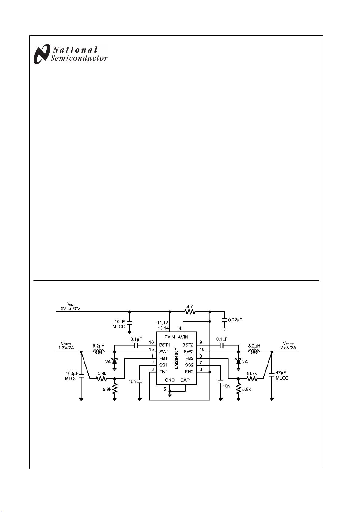
Typical Application
20200252
© 2007 National Semiconductor Corporation 202002 www.national.com
LM26400Y Dual 2A, 500kHz Wide Input Range Buck Regulator
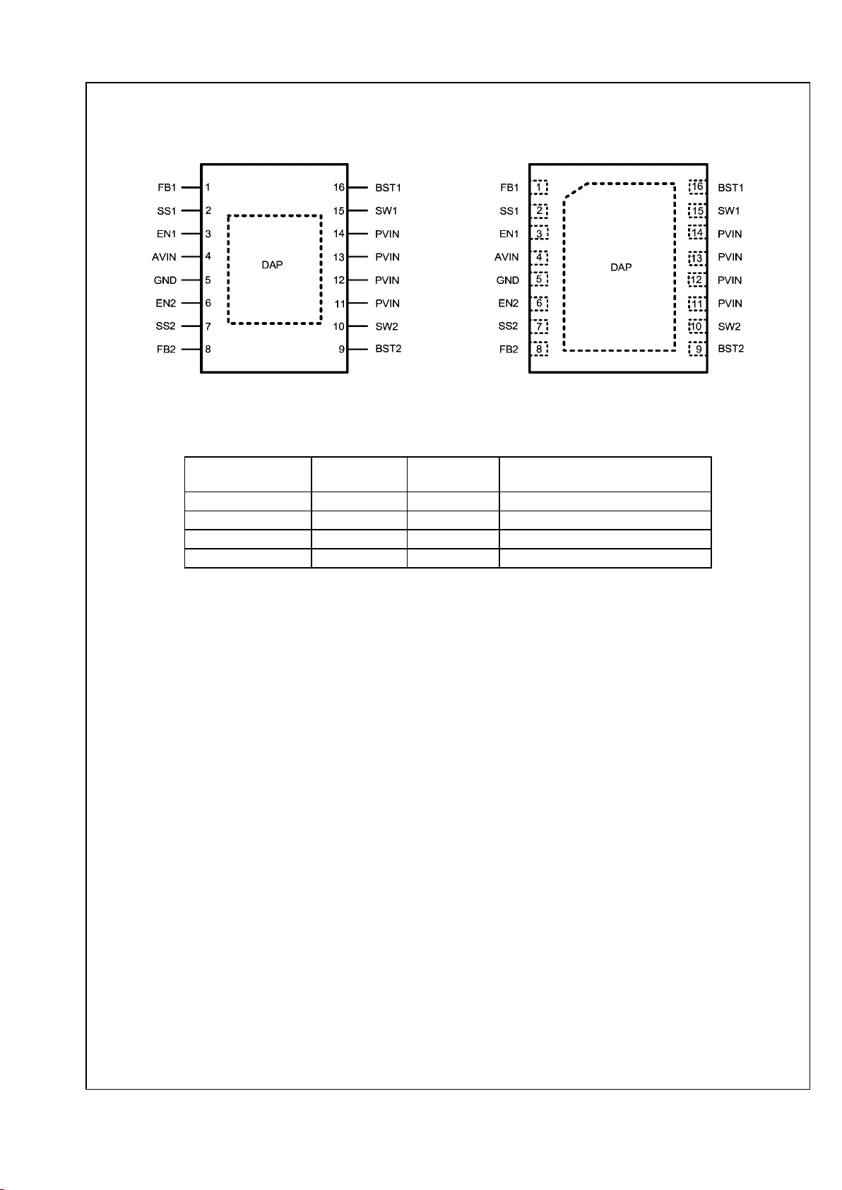
Connection Diagrams
16-Lead ETSSOP (top view)
20200202
NS Package Drawing MXA16A
16-Lead LLP (top view)
20200203
NS Package Drawing SDA16A
Ordering Information
Order Number Package Type
NSC Package
Drawing
Supplied As
LM26400YMH ETSSOP-16 MXA16A Rail of 92 Units
LM26400YMHX ETSSOP-16 MXA16A 2500 Units on Tape and Reel
LM26400YSD LLP-16 SDA16A 1000 Units on Tape and Reel
LM26400YSDX LLP-16 SDA16A 4500 Units on Tape and Reel
www.national.com 2
LM26400Y
Pin Descriptions
Pin Name Description
1 FB1
Feedback pin of Channel 1. Connect FB1 to an external voltage divider to set the
output voltage of Channel 1.
2 SS1
Soft start pin of Channel 1. Connect a capacitor between this pin and ground to
program the start up speed.
3 EN1
Enable control input for Channel 1. Logic high enables operation. Do not allow this
pin to float or be greater than VIN + 0.3V.
4 AVIN
Input supply for generating the internal bias used by the entire IC and for generating
the internal bootstrap bias. Needs to be locally bypassed.
5 GND
Signal and Power ground pin. Kelvin connect the lower resistor of the feedback
voltage divider to this pin for good load regulation.
6 EN2
Enable control input for Channel 2. Logic high enables operation. Do not allow this
pin to float or be greater than VIN + 0.3V.
7 SS2
Soft start pin of Channel 2. Connect a capacitor between this pin and ground to
program the start up speed.
8 FB2
Feedback pin of Channel 2. Connect FB2 to an external voltage divider to set the
output voltage of Channel 2.
9 BST2
Supply rail for the gate drive of Channel 2's NMOS switch. A bootstrap capacitor
should be placed between the BST2 and SW2 pins.
10 SW2
Switch node of Channel 2. Connects to the inductor, catch diode, and bootstrap
capacitor.
11, 12, 13,14 PVIN
Input voltage of the power supply. Directly connected to the drain of the internal
NMOS switch. Tie these pins together and connect to a local bypass capacitor.
15 SW1
Switch node of Channel 1. Connects to the inductor, catch diode, and bootstrap
capacitor.
16 BST1
Supply rail for the gate drive of Channel 1's NMOS switch. A bootstrap capacitor
should be placed between the BST1 and SW1 pins.
DAP Die Attach Pad
Must be connected to system ground for low thermal impedance and low grounding
inductance.
3 www.national.com
LM26400Y
Absolute Maximum Ratings (Note 1)
If Military/Aerospace specified devices are required,
please contact the National Semiconductor Sales Office/
Distributors for availability and specifications.
AVIN, PVIN −0.5V to 22V
SWx Voltage −0.5V to 22V
BSTx Voltage −0.5V to 26V
BSTx to SW Voltage −0.5V to 6V
FBx Voltage −0.5V to 3V
ENx Voltage (Note 2) −0.5V to 22V
SSx Voltage −0.5V to 3V
Junction Temperature +150°C
ESD Susceptibility
Human Body Model (Note 3) 2kV
Storage Temperature Range -65°C to 150°C
Operating Ratings (Note 1)
V
IN
3V to 20V
Junction Temperature −40°C to +125°C
Electrical Characteristics
Unless otherwise stated, the following conditions apply: AVIN = PVIN = VIN = 5V. Limits in standard type are for TJ = 25°C only;
limits in boldface type apply over the junction temperature (TJ) range of -40°C to 125°C. Minimum and Maximum limits are
guaranteed through test, design, or statistical correlation. Typical values represent the most likely parametric norm at TJ = 25°C,
and are provided for reference purposes only.
Symbol Parameter Conditions Min Typ Max Units
V
FB
Voltages at FB1 and FB2 Pins
0°C to 85°C. Feedback Loop Closed. 0.591
0.6
0.611
V
-40°C to 125°C. Feedback Loop
Closed.
0.585 0.617
ΔV
FB_LINE
Line Regulation of FB1 and FB2
Voltages, Expressed as PPM
Change Per Volt of V
IN
Variation
VIN = 3V to 20V
66 ppm/V
I
FB
Current in FB1 and FB2 Pins
VFB = 0.6V
0.4 250 nA
V
UVLO
Under Voltage Lockout
Threshold
VIN Rises From 0V
2.7 2.9
V
VIN Falls From 3.3V
2.0 2.3
V
UVLO_HYS
Hysteresis of UVLO Threshold 0.2 0.36 0.55 V
f
SW
Switching Frequency 0.39 0.52 0.65 MHz
D
MAX
Maximum Duty Cycle 90 96 %
D
MIN
Minimum Duty Cycle 2 %
R
DS_ON
ON Resistance of Internal
Power MOSFET
ETSSOP, 2A Drain Current 175 320
mΩ
LLP, 2A Drain Current 194 350
I
CL
Peak Current Limit of Internal
MOSFET
2.5 3 4.5 A
I
SD
Shutdown Current of AVIN Pin EN1 = EN2 = 0V 2 nA
I
Q
Quiescent Current of AVIN Pin
(both channels are enabled but
not switching)
EN1 = EN2 = 5V, FB1 = FB2 = 0.7V 4 mA
V
EN_IH
Input Logic High of EN1 and
EN2 Pins
2.5 V
V
EN_IL
Input Logic Low of EN1 and
EN2 Pins
0.4 V
I
EN
EN1 and EN2 Currents (sink or
source)
5 nA
I
SW_LEAK
Switch Leakage Current
Measured at SW1 and SW2
Pins
EN1 = EN2 = SWx = 0 1 µA
ΔΦ
Phase Shift Between SW1 and
SW2 Rising Edges
Feedback Loop Closed. Continuous
Conduction Mode.
170 180 190 deg
I
SS
SSx Pin Current 11 16 21 µA
www.national.com 4
LM26400Y
Symbol Parameter Conditions Min Typ Max Units
ΔI
SS
Difference Between SS1 and
SS2 Currents
3 µA
V
FB_F
FB1 and FB2 Frequency Foldback Threshold
0.35 V
Thermal Characteristics
Symbol Description Conditions
Typical Value
Unit
TSSOP LLP
θ
JA
Junction-to-Ambient Thermal
Resistance (Note 4)
Mount package on a standard board (Note 5) and
test per JESD51-7 standard.
28 26
°C/W
θ
JC
Junction-to-Case-Bottom
Thermal Resistance
3 2.8
T
SD
Thermal Shutdown
Threshold
Junction temperature rises. 165
°C
T
SD_HYS
Thermal Shutdown
Hysteresis
Junction temperature falls from above TSD.
15
Note 1: Absolute maximum ratings indicate limits beyond which damage to the device may occur. Operating Ratings are conditions under which the device is
intended to be functional, but specific performance is not guaranteed. For guaranteed performance limits and associated test conditions, see Electrical
Characteristics table.
Note 2: EN1 and EN2 pins should never be higher than VIN + 0.3V.
Note 3: The human body model is a 100pF capacitor discharged through a 1.5 kΩ resistor into each pin. Test method is per JESD-22-A114.
Note 4: Value is highly board-dependent. For comparison of package thermal performance only. Not recommended for prediction of junction temperature in real
applications. See THERMAL CONSIDERATIONS for more information.
Note 5: A standard board refers to a four-layer PCB with the size 4.5”x3”x0.063”. Top and bottom copper is 2 oz. Internal plane copper is 1 oz. For details refer
to JESD51-7 standard.
5 www.national.com
LM26400Y
Typical Performance Characteristics Unless otherwise specified or thermal-shutdown related, T
A
= 25°
C for efficiency curves, loop gain plots and waveforms, and TJ = 25°C for all others.
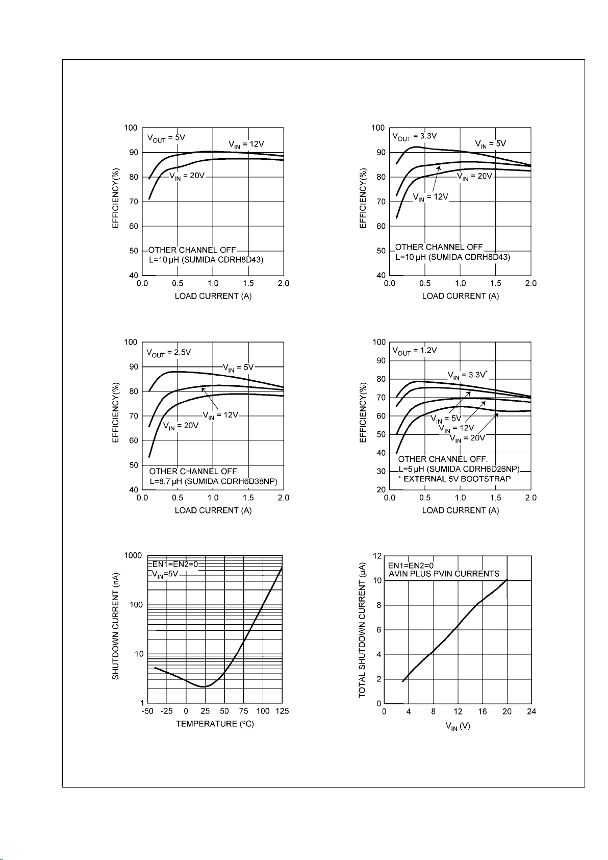
Efficiency, V
OUT
= 5V
20200237
Efficiency, V
OUT
= 3.3V
20200216
Efficiency, V
OUT
= 2.5V
20200217
Efficiency, V
OUT
= 1.2V
20200218
AVIN Shutdown Current vs. Temperature
20200206
VIN Shutdown Current vs. V
IN
20200238
www.national.com 6
LM26400Y
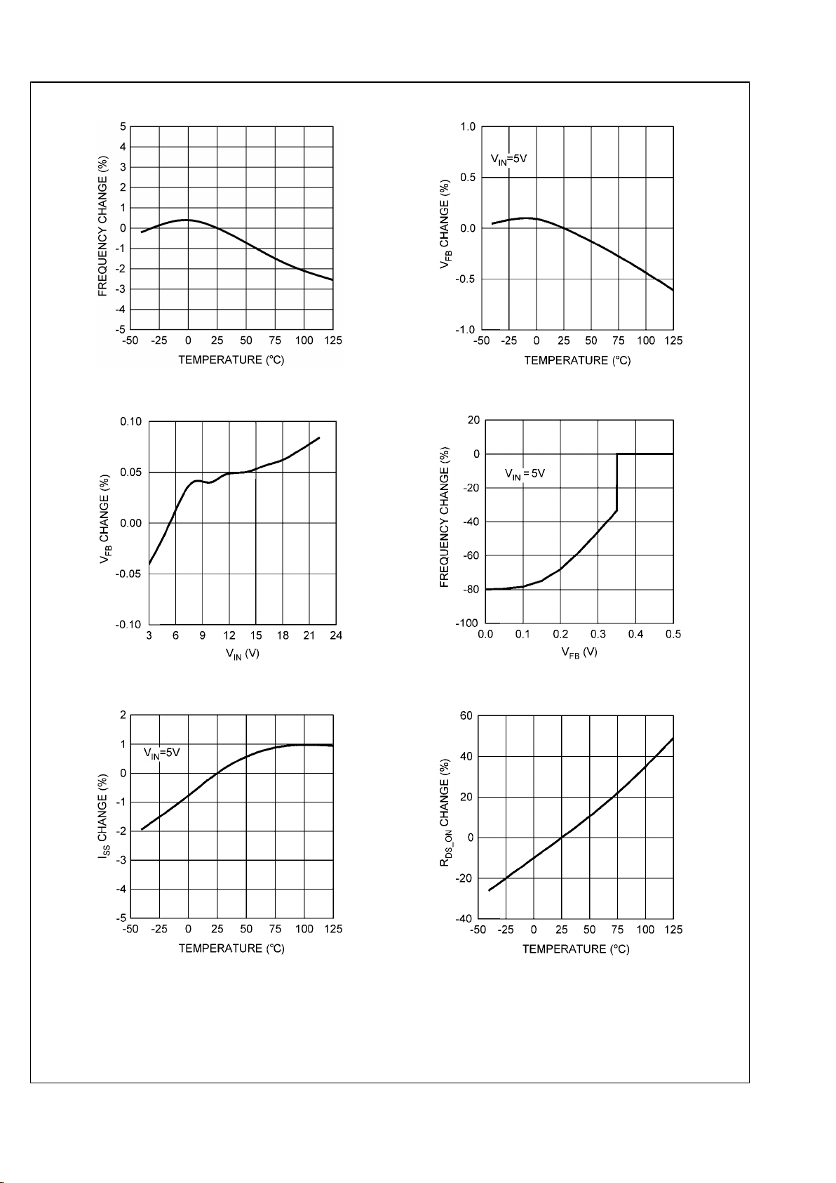
Switching Frequency vs. Temperature
20200207
Feedback Voltage vs. Temperature
20200208
Feedback Voltage vs. V
IN
20200209
Frequency Foldback
20200210
SS-Pin Current vs. Temperature
20200278
FET R
DS_ON
vs. Temperature
20200221
7 www.national.com
LM26400Y
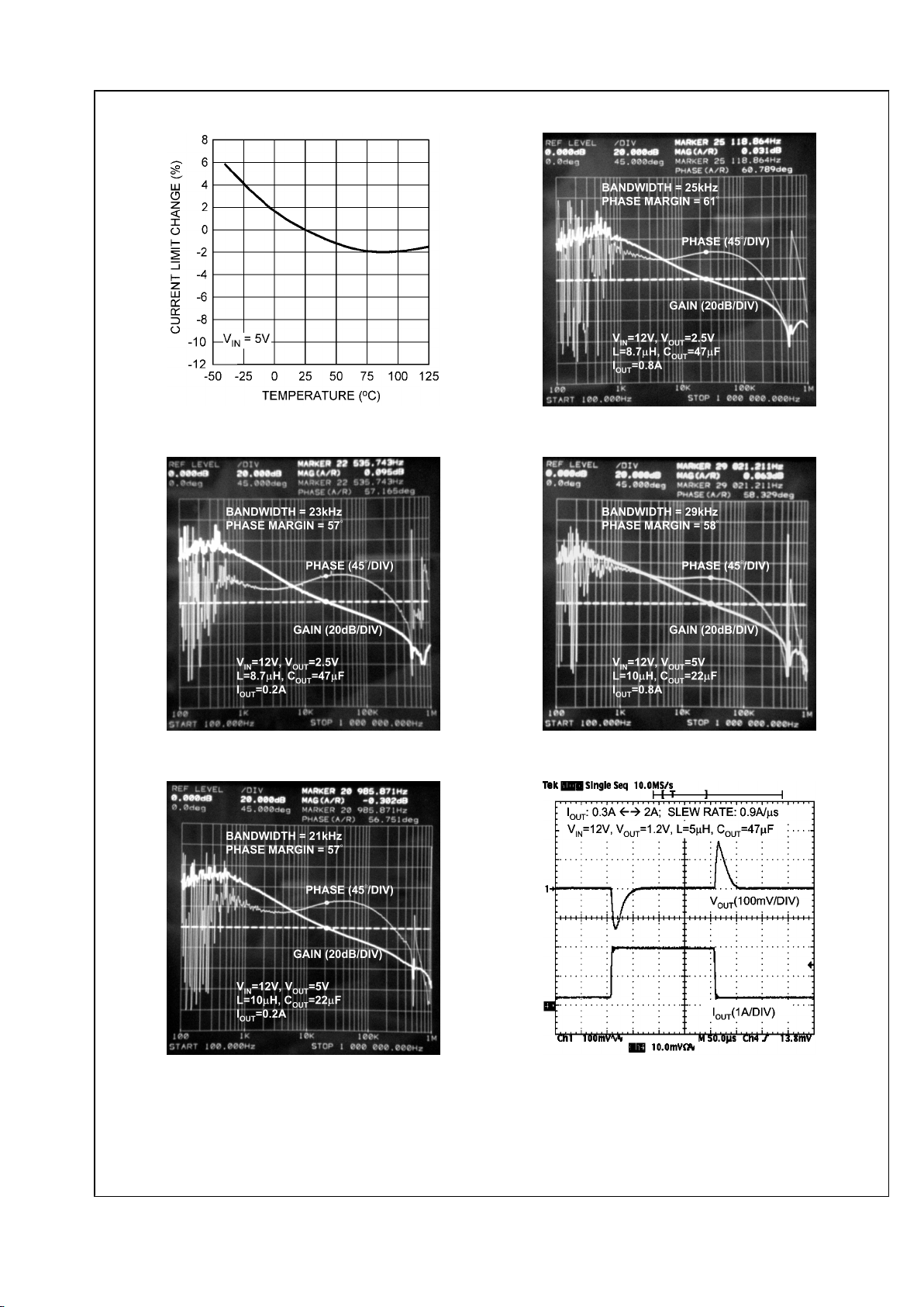
Switch Current Limit vs. Temperature
20200234
Loop Gain, CCM
20200219
Loop Gain, DCM
20200220
Loop Gain, CCM
20200236
Loop Gain, DCM
20200222
Load Step Response
20200223
www.national.com 8
LM26400Y
 Loading...