

NSC LM2639MX, LM2639M, LM2639EVAL Datasheet
LM2639
5-Bit Programmable, High Frequency Multi-phase PWM
Controller
General Description
The LM2639 provides an attractive solution for power supplies of high power microprocessors (such as Pentium II
™
,
MII
™
,K6™-2, K6™-3, etc.) exhibiting ultra fast load transients. Compared to a conventional single-phase supply, an
LM2639 based multi-phase supply distributes the thermal
and electrical loading amongcomponentsin multiple phases
and greatly reduces the corresponding stress in each component. The LM2639 can be programmed to control either a
3-phase converter or a 4-phase converter. Phase shift
among the phases is 120˚ in the case of three phase and 90˚
with four-phase. Because the power channels are out of
phase, there can be significant ripple cancellation for both
the input and output current, resulting in reduced input and
output capacitor size. Due to the nominal operating frequency of 2 MHz per phase, the size of the output inductors
can be greatly reduced which results in a much faster load
transient response and a dramatically shrunk output capacitor bank. Microprocessor power supplies with all surface
mount components can be easily built.
The internal high speed transconductance amplifier guarantees good dynamic performance. The output drive voltages
can be adjusted through a resistor divider to control switching loss in the external FETs.
The internal master clock frequency of up to 8 MHz is set by
an external reference resistor. An external clock of 10 MHz
can also be used to drive the chip to achieve frequency control and multi-chip operation.
The LM2639 also provides input under-voltage lock-out with
hysteresis and input over-current protection.
Features
n Ultra fast load transient response
n Enables all surface-mount-design
n Selectable 2, 3, 4 phase operation
n Clock frequency from 40 kHz to 10 MHz
n Precision load current sharing
n 5-bit programmable from 3.5V to 1.3V
n VID code compatible to VRM 8.X specification
n Output voltage is 2.0V for VID code 11111
n Selectable internal or external clock
n Digital 16-step soft start
n Input under-voltage lock-out, over-current protection
Applications
n Servers and workstations
n High current, ultra-fast transient microprocessors
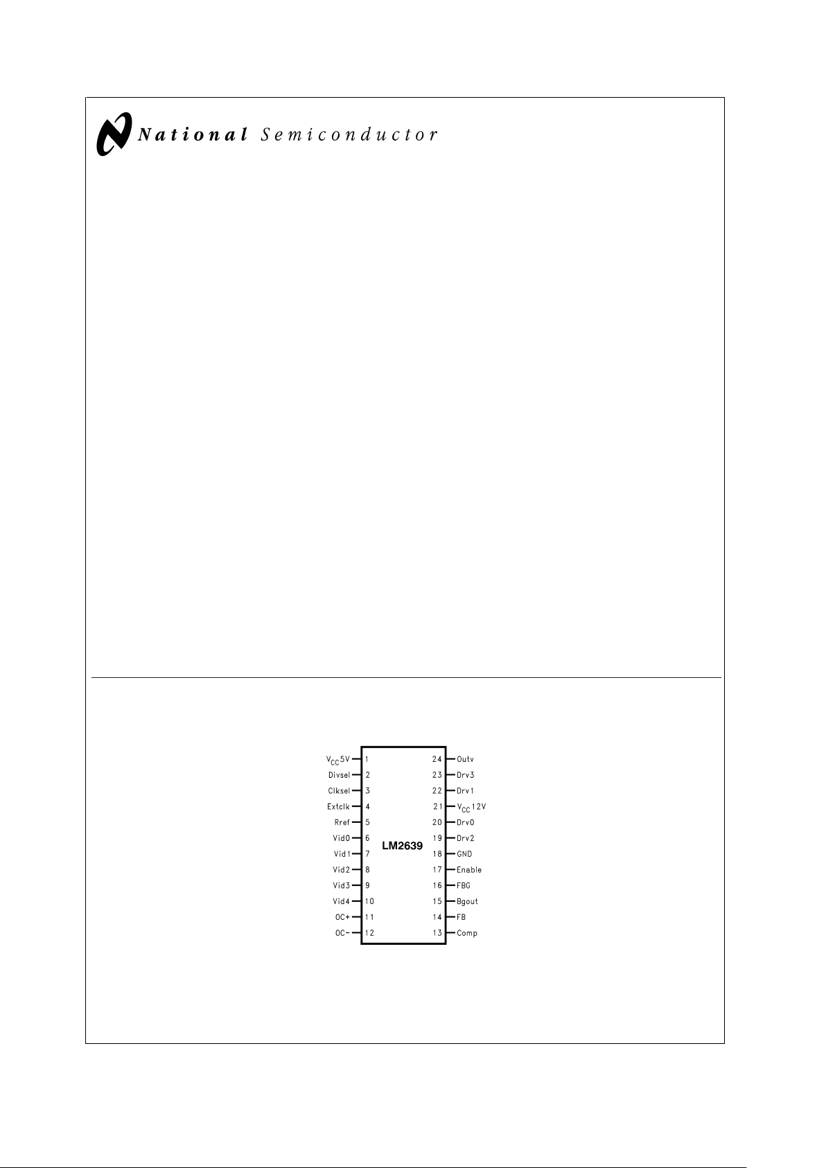
Pin Configuration
MII™is a trademark of Cyrix Corporation a wholly owned subsidiary of National Semiconductor Corporation.
Pentium II
™
is a trademark of Intel Corporation.
K6
™
is a trademark of Advanced Micro Devices, Inc.
24-Pin Plastic SOIC
DS101143-1
Top View
See NS Package Number M24B
February 2000
LM2639 5-Bit Programmable, High Frequency Multi-phase PWM Controller
© 2000 National Semiconductor Corporation DS101143 www.national.com
Absolute Maximum Ratings (Note 1)
If Military/Aerospace specified devices are required,
please contact the National Semiconductor Sales Office/
Distributors for availability and specifications.
V
CC
5V 7V
V
CC
12V 20V
Junction Temperature 125˚C
Power Dissipation (Note 2) 1.6W
Storage Temperature −65˚C to +150˚C
ESD Susceptibility (Note 8) 2 kV
Soldering Time, Temperature 10 sec., 300˚C
Operating Ratings (Note 1)
V
CC
4.75V to 5.25V
Junction Temperature Range 0˚C to 70˚C
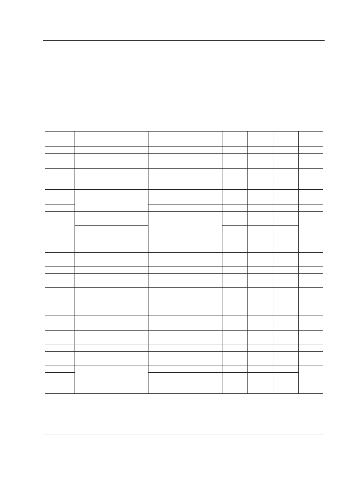
Electrical Characteristics
VCC5V=5V, VCC12V=12V unless otherwise specified. Typicals and limits appearing in plain type apply for T
A
=
T
J
=
+25˚C.
Limits appearing in boldface type apply over the entire operating temperature range.
Symbol Parameter Conditions Min Typ Max Units
Vcc5V V
CC
5V Pin Voltage 4.5 5.0 5.5 V
Vcc12V V
CC
12V Pin Voltage 10.0 12.0 18.0 V
V
DACOUT
5-bit DAC Output Voltage (Note 3)
N
−1
%
NN
+1
%
V
N
−1.5
%
NN
+1.5
%
I
CC
12V Quiescent VCC12V Current Enable=5V, VID=00001,
DRV Outputs Floating
1.3 3 mA
I
CC
5V Operating VCC5V Current V
OUT
=
2.00V 4.3 8 mA
V
REF
Rref Pin Voltage 1.225 V
V
INL
Vid0:4, Clksel, Divsel, and
Enable Pins Logic Threshold
Logic Low (Note 4) 1.8 1.5 V
V
INH
Logic High (Note 5) 3.5 2.8 V
I
INL
Vid0:4 and Enable Pins Internal
Pullup Current
The Corresponding Pin=0V
60 100 140
µA
Clksel, Divsel Pins Internal
Pullup Current
−10 0 10
Gate Driver Resistance When
Sinking Current
I
SINK
=
50 µA, V
CC
12V=14V 12 Ω
V
DRV
DRV0:3 Output Voltage I
DRV
=
10 mA, V
CC
12V=14V,
OutV=12V or 5V
OutV −
0.3V
OutV OutV +
0. 3V
V
t
fall
DRV0:3 Fall Time (Note 6) 7 ns
I
SRC
DRV0:3 Source Current DRV0:3=0V, VCC12V=14V,
OutV=5V
40 60 mA
I
SINK
DRV0:3 Sink Current DRV0:3=5V, VCC12V=14V,
OutV=5V
90 160 250 mA
B
gOUT
Voltage Current Limit Not Activated 4
V
Current Limit Activated 0
I
FB
FB Pin Bias Current FB=2V 30 nA
B
gOUT
Sink Current B
gOUT
=
1V 1.0 2.4 5 mA
F
OSC
Oscillator Frequency 8.02kΩ from Rref Pin to
Ground
7.0 8.0 8.7 MHz
∆
D
DRV0:3 Duty Cycle Match Duty Cycle=50
%
−1 +1
%
∆
ph
DRV0:3 Phase Accuracy Duty Cycle=50%,F
clock
=
8
MHz
−1 +1 Deg
T
off
PWM Off time
Divide by 4 22
%
T
off
Divide by 3 22
OutV Drive Voltage Range Output Freq.=2MHz, V
O
=
2.00V
0 12 Vcc12 V
LM2639
www.national.com 2
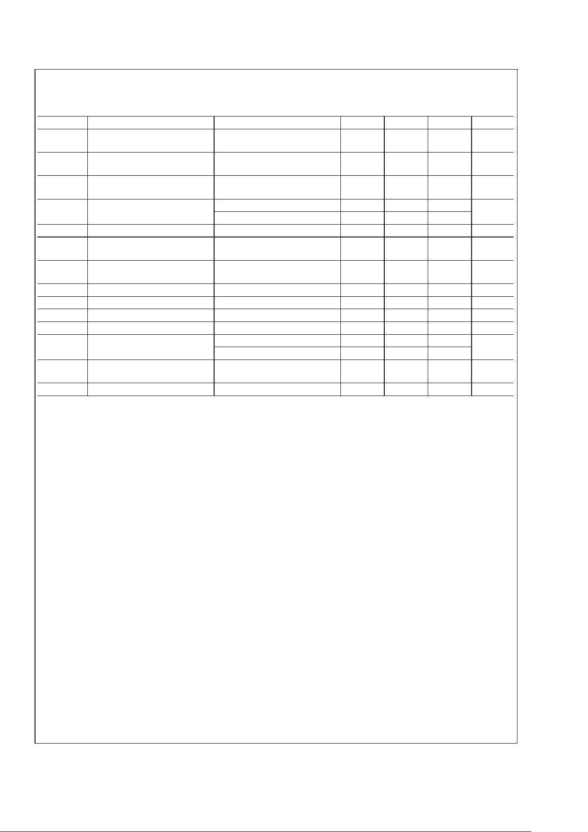
Electrical Characteristics (Continued)
VCC5V=5V, VCC12V=12V unless otherwise specified. Typicals and limits appearing in plain type apply for T
A
=
T
J
=
+25˚C.
Limits appearing in boldface type apply over the entire operating temperature range.
Symbol Parameter Conditions Min Typ Max Units
V
OCC_CM
Over-current Comparator
Common Mode Range
312V
IB_OC+ OC+ Input Bias Current V
IN
=
5V, OC+=5V, OC−
=
4V
100 145 200 µA
IB_OC− OC− Input Bias Current V
IN
=
5V, OC+=6V, OC−
=
5V
85 125 165 µA
V
OS_OCC
Over-current Comparator Input
Offset Voltage
V
IN
=
5V 2 16 42
mV
V
IN
=
12V 21
D
MAX
Maximun Duty Cycle FB=0V 78
%
gm Error Amplifier
Transconductance
1.36 mmho
V
ramp
Ramp Signal Peak-to-Peak
Amplitude
2V
I
comp
COMP Pin Source Current 250 400 550 µA
I
comp
COMP Pin Sink Current 160 280 400 µA
V
comp_hi
COMP Pin High Clamp 2.9 V
V
comp_lo
COMP Pin Low Clamp 0.19 V
V
POR
Power On Reset Trip Point Vcc5V Pin Voltage Rising 4.0
V
Vcc5V Pin Voltage Falling 3.6
Vcc12V Minimum Working
Voltage
(Note 7) 3.8 V
t
SS
Soft Start Delay F
OSC
=
8MHz 1.6 ms
Note 1: Absolute Maximum Ratings are limits beyond which damage to the device may occur. Operating ratings do not imply guaranteed performance limits.
Note 2: Maximum allowable power dissipation is a function of the maximum junction temperature, T
JMAX
, the junction-to-ambient thermal resistance, θJA, and the
ambient temperature, T
A
. The maximum allowable power dissipation at any ambient temperature is calculated using:
P
MAX
=
(T
JMAX−TA
)/
θ
JA
.
The
junction-to-ambient thermal resistance, θ
JA
, for LM2639 is 78˚C/W. For a T
JMAX
of 150˚C and TAof 25˚C, the maximum allowable power dissipation is 1.6W.
Note 3: The letter
N
stands for the typical output voltages appearing in
italic boldface
type in
Table 1
.
Note 4: Maxvalue of logic low means any voltage below this value is guaranteed to be taken as logic low whereas a voltage higher than this value is not guaranteed
to be taken as a logic low.
Note 5: Minvalueof logic high means any voltage above this value is guaranteed to be taken as logic high whereas a voltage lower than this value is not guaranteed
to be taken as a logic high.
Note 6: When driving bipolar FET drivers in the typical application circuit.
Note 7: When Vcc12V pin goes below this voltage, all DRV pins go to 0V.
Note 8: ESD ratings for pins DRV0, DRV1, DRV2 and DRV3 is 1kV. ESD rating for all other pins is 2kV.
LM2639
www.national.com3
 Loading...