


LM2638
Motherboard Power Supply Solution with a 5-Bit
Programmable Switching Controller and Two Linear
Regulator Controllers
General Description
The LM2638 provides a comprehensive embedded power
supply solution for motherboards hosting high performance
MPUs suchas Pentium
™
II,MII™,K6™-2 and other similar
high performance MPUs. The LM2638 incorporates a 5-bit
programmable, synchronous buck switching controller and
two high-speed linear regulator controllers in a 24-pin SO
package. In a typical application, the switching controller
supplies the MPU core, and the linear regulator controllers
supply the GTL+ bus and the clock or graphics chip core. A
charge pump pin helps provide the necessary voltage to
power the linear sections when 12V isshut off during system
standby such as STR mode.
Switching Section
— The switching regulator controller features an Intel-compatible, 5-bit programmable output voltage, over-current and over-voltage protection, a power good
signal, and a logic-controlled output enable. There are two
user-selectable over-current protection methods. One provides accurate over-current protection with the use of an external sense resistor. The other saves cost by taking advantage of the r
DS_ON
of the high-side FET. When there is an
over voltage, the controller turns off the high side FET and
turns on the low side.
Linear Section
— The two linear regulator controllers feature wide control bandwidth, N-FETand NPN transistor driving capability and an adjustable output. The wide control
bandwidth makes meeting the GTL+ bus transient response
requirement an easy job. In minimum configuration, the two
controllers default to 1.5V and 1.25V respectively.
Both linear controllers have under voltage latch-off.
Features
n Provides 3 regulated voltages
n Power Good flag and output enable
n Charge pump pin
Switching Section
n Synchronous rectification
n 5-bit DAC programmable down to 1.3V
n Typical
±
1%DAC tolerance
n Switching frequency: 50 kHz to 1 MHz
n Over-voltage protection
n Two methods of over-current protection
n Adaptive non-overlapping FET gate drives
n Soft start without external capacitor
Linear Section
n N-FET and NPN drive capability
n Ultra fast response speed
n Under voltage latch-off at 0.63V
n Output voltages default to 1.5V and 2.5V yet adjustable
Applications
n Embedded power supplies for motherboards
n Triple DC/DC power supplies
n Programmable high current DC/DC power supply
Pin Configuration
MII™is a trademark of Cyrix Corporation a wholly owned subsidiary of National Semiconductor Corporation.
Pentium
™
is a trademark of Intel Corporation.
K6
™
is a trademark of Advanced Micro Devices, Inc.
24-Lead SOIC
DS101034-1
Top View
Order Number LM2638M
See NS Package Number M24B
May 1999
LM2638 Motherboard Power Supply Solution with a 5-Bit Programmable Switching Controller and
Two Linear Regulator Controllers
© 1999 National Semiconductor Corporation DS101034 www.national.com
Absolute Maximum Ratings (Note 1)
If Military/Aerospace specified devices are required,
please contact the NationalSemiconductor Sales Office/
Distributors for availability and specifications.
V
CC
7V
V
DD
17V
Junction Temperature 150˚C
Power Dissipation (Note 2) 1.6W
Storage Temperature −65˚C to +150˚C
ESD Susceptibility 3 kV
Soldering Time, Temperature (10 sec.) 300˚C
Operating Ratings (Note 1)
V
CC
4.75V to 5.25V
Junction Temperature Range 0˚C to +125˚C
Electrical Characteristics V
CC
=
5V, V
DD
=
12V unless otherwise specified. Typicals and limits appearing in
plain type apply for T
A
=
T
J
=
+25˚C. Limits appearing in boldface type apply over the 0˚C to +70˚C range.
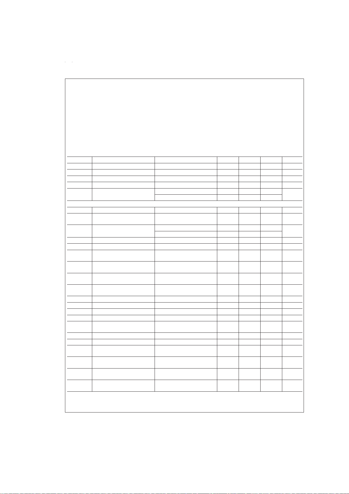
Symbol Parameter Conditions Min Typ Max Units
I
EN
EN Pin Internal Pull-up Current 60 90 140 µA
I
CC
Operating VCCCurrent EN=5V, VID=10111 6 7.5 mA
I
Q_VCC
VCCShutdown Current EN=0V, VID Pins Floating 1.5 3 mA
I
Q_VDD
VDDShutdown Current EN=0V, VID Pins Floating 4 µA
R
DS_CP
CP Pin Resistance High Side FET 100
Ω
Low Side FET 10
SWITCHING SECTION
V
DACOUT
5-Bit DAC Output Voltage (Note 3)
N
−1.5
%
NN
+1.5
%
V
I
VID
VID Pins Internal Pull-up
Current
60 90 140 µA
f
OSC
Oscillator Frequency RT=100 kΩ 204 245 286
kHz
RT=25 kΩ 1000
D
MAX
Maximum Duty Cycle 100
%
D
MIN
Minimum Duty Cycle 0
%
R
SNS1
SNS1 Pin Resistance to
Ground
8.5 10 13 kΩ
R
DS_SRC
Gate Driver Resistance When
Sourcing Current
6 Ω
R
DS_SINK
Gate Driver Resistance When
Sinking Current
1.5 Ω
V
CC_TH1
VCCPower-On-Reset
Threshold
4.0 4.3 V
V
CC_TH2
VCCShutdown Threshold 3.0 3.6 V
V
DAC_IH
DAC Input High Voltage 3.5 V
V
DAC_IL
DAC Input Low Voltage 1.3 V
GA Error Amplifier DC Gain 76 dB
BW
EA
Error Amplifier Unity Gain
Bandwidth
5 MHz
V
RAMP_L
Ramp Signal Valley Voltage 1.25 V
V
RAMP_H
Ramp Signal Peak Voltage 3.25 V
t
SS
Soft Start Time
4096
Clock
Cycles
D
STEP_SS
Duty Cycle Step Change during
Soft Start
12.5
%
t
PWGD
PWGD Response Time SNS1 Rises from 0V to Rated
Output Voltage
2 8.4 15 µs
t
PWBAD
PWGD Response Time SNS1 Falls from Rated Output
Voltage to 0V
2 3.4 10 µs
www.national.com 2

Electrical Characteristics V
CC
=
5V, V
DD
=
12V unless otherwise specified. Typicals and limits appearing in
plain type apply for T
A
=
T
J
=
+25˚C. Limits appearing in boldface type apply over the 0˚C to +70˚C range. (Continued)
Symbol Parameter Conditions Min Typ Max Units
SWITCHING SECTION
V
PWGD_HI
PWGD High Trip Point
%
Above Rated Output Voltage
When Output Voltage
↑
11.5 13
%
%
Above Rated Output Voltage
When Output Voltage
↓
(Note
4)
5 7 9
V
PWGD_LO
PWGD Low Trip Point
%
Below Rated Output Voltage
When Output Voltage
↑
2.6 6
%
%
Below Rated Output Voltage
When Output Voltage
↓
(Note
4)
6 9.5 13
V
OVP_TRP
Over-Voltage Trip Point
%
SNS1 Above Rated Output 15 25 35
%
I
CS+
CS+ Pin Sink Current CS+=5V, CS−=4.8V 126 185 244 µA
V
OCP
Over-Current Trip Point (CS+
and CS− Differential Voltage)
CS+=2V, CS− Drops from 2V
41 55 69 mV
1.5V LDO CONTROLLER SECTION
V
SNS2
SNS2 Voltage V
DD
=
12V, V
CC
=
4.75V to
5.25V, I
G2
=
0mAto20mA
1.463 1.5 1.538 V
R
OUT2
Output Resistance 200 Ω
I
SNS2
SNS2 Pin Bias Current When Regulating 21 µA
V
PWGD_HI
PWGD High Trip Point (Note 4) 0.63 V
V
PWGD_LO
PWGD Low Trip Point (Note 4) 0.44 V
1.25V LDO CONTROLLER SECTION
V
SNS3
SNS3 Voltage V
DD
=
12V, V
CC
=
4.75V to
5.25V, I
G3
=
0mAto20mA
1.219 1.25 1.281 V
R
OUT3
Output Resistance 200 Ω
I
SNS3
SNS3 Pin Bias Current When Regulating 0 µA
V
PWGD_HI
PWGD High Trip Point (Note 4) 0.63 V
V
PWGD_LO
PWGD Low Trip Point (Note 4) 0.44 V
Note 1: Absolute Maximum Ratings are limits beyondwhichdamageto the device may occur.Operatingratings are conditions under which the device operates
correctly. Operating Ratings do not imply guaranteed performance limits.
Note 2: Maximum allowable power dissipation is a function of the maximum junction temperature, T
JMAX
, the junction-to-ambient thermal resistance, θJA, and the
ambient temperature, T
A
. The maximum allowable power dissipation at any ambient temperature is calculated using:
P
MAX
=
(T
JMAX−TA
)/
θ
JA
.
The
junction-to-ambient thermal resistance, θ
JA
, for LM2638 is 78˚C/W. For a T
JMAX
of 150˚C and TAof 25˚C, the maximum allowable power dissipation is 1.6W.
Note 3: The letter
N
stands for the typical output voltages appearing in
italic boldface
type in
Table 1
.
Note 4: The output level of the PWGD pin is a logic AND of the power good function of the switching section, the 1.5V section and the 1.25V section. Fortheswitching section, the power good is a window. For the two linear sections, the power good is a threshold with some hysteresis.
www.national.com3
 Loading...