

NSC LM2630MTCX-ADJ, LM2630MTC-ADJ Datasheet
LM2630
Synchronous Step-Down Power Supply Controller
General Description
The LM2630 controller provides all the active functions for
step-down (buck)switching converters. These dc-to-dc converters provide core CPU power in battery-operated systems.
High efficiency is achieved by using synchronous rectification and pulse-skipping mode operation at light load. Inexpensive N-channel MOSFETs are used to reduce system
cost. Bootstrap circuit is used to drive the high-side
N-channel MOSFET.
Current mode control schemeis used to improve line regulation and transient response, also provides cycle-by-cycle
current limiting.
The operating frequency is adjustable between 200 kHz and
400 kHz. An external shutdown pin can be used to disable
the device and reducethe quiescent current to 0.1µA. In low
noise applications, bringing theFPWMpin high can force the
device to operate in constant frequency mode. Other features include the external synchronization pin, and the
PGOOD pin to indicate the state of the output voltage.
Protection circuitry includesthermal shutdown, undervoltage
shut down, soft-startcapability,and two levelsof current limits: The first levelsimply limits the load currentdirectly; at the
second level, if the load pulls the output voltage down below
80%of the regulated value, the chip willshut down. This
latched operation is disabled during startup, but an internal
timer will enable it if the outputdoes not come up in the preset time.
Features
n 4.5V to 30V input range
n Adjustable output (1.8V to 6V)
n 200 kHz to 400 kHz adjustable operating frequency
n Externally synchronizable
n On-board power good function
n Precision 1.24V reference output
n 0.8 mA typical quiescent current
n 0.1 µA shutdown current
n Thermal shutdown
n Direct current limit protection
n Input undervoltage lockout
n Output Undervoltage shutdown protection
n Programmable soft-start function
n Tiny TSSOP package
Applications
n Notebook and subnotebook computers
n Cellular phones
n Portable instruments
n Battery-powered digital devices
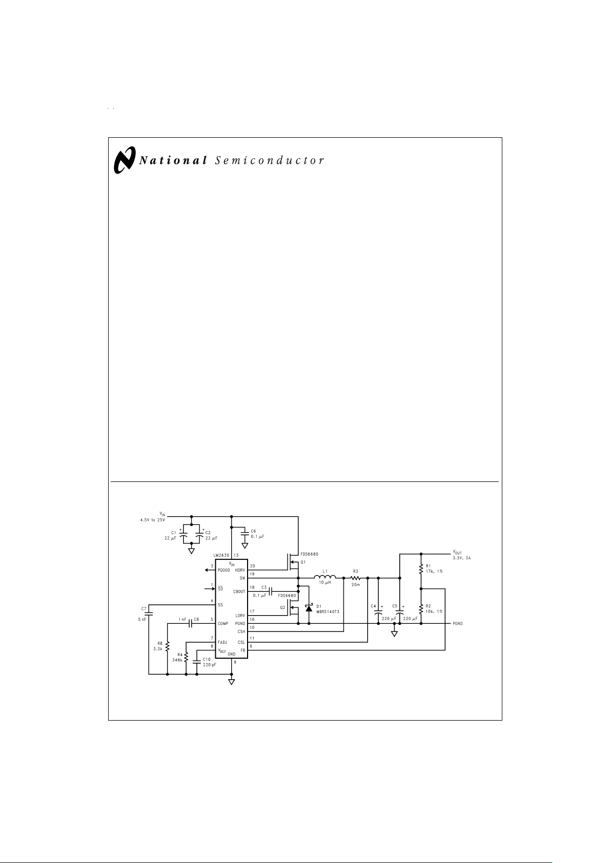
Typical Application Circuit
DS100120-1
February 1999
LM2630 Synchronous Step-Down Power Supply Controller
© 1999 National Semiconductor Corporation DS100120 www.national.com
Absolute Maximum Ratings (Note 1)
If Military/Aerospace specified devices are required,
please contact the NationalSemiconductorSales Office/
Distributors for availability and specifications.
Voltages from the indicated
pins to GND and PGND:
V
IN
−0.3V to 31V
CBOOT −0.3V to 36V
SD
−0.3V to 31V
SW −0.3V to 31V
CSH, CSL −0.3V to 7V
FPWM, SYNC −0.3V to 10V
Power Dissipation (T
A
=
70˚C), (Note 2)
720mW
Storage Temperature Range −65˚C to +150˚C
Soldering Dwell Time,
Temperature (Note 3)
Wave 4 sec, 260˚C
Infrared 10 sec, 240˚C
Vapor Phase 75 sec, 219˚C
ESD Rating (Note 4) 1.5 kV
Operating Ratings
V
IN
4.5V to 30V
Junction Temperature −40˚C to +125˚C
Electrical Characteristics
Specifications in standard type face are for T
j
=
25˚C and those with boldface type apply over full operating junction tem-
perature range. V
IN
=
10V, GND=PGND=0V,unless otherwise stated. (Notes 5, 6)
Symbol Parameter Conditions Typical Limit Units
System
V
IN
Input Supply Voltage 4.5
30
V(min)
V(max)
V
OUT
Output Voltage Adjustment
Range
1.8
6.0
V(min)
V(max)
∆V
OUT
/
V
OUT
Load Regulation 0 mV ≤ (CSH-CSL) ≤ 75 mV
0.3
%
∆V
OUT
/
V
OUT
Line Regulation 4.5 ≤ VIN≤ 30V
0.002
%
/V
I
IN
Input Supply Current with the
Switching Controller ON
V
FB
=
1V, V
CSH
=
2.15V, V
CSL
=
2.1V
0.8 mA
1.2/1.4 mA(max)
Input Supply Current with the
Switching Controller ON
(Internal Rail is Supplied
from CSL Pin)
V
FB
=
1V, V
CSH
=
5.15V, V
CSL
=
5V
0.15 mA
Input Supply Current with the
IC Shut Down
V
SD
=
0V, V
IN
=
30V
0.1 µA
3 (Note 7) µA(max)
Minimum Output Voltage for
CSL Providing the Internal
Rail
3V
I
SS
Soft Start Source Current V
SS
=
1.5V 10 µA
5 µA(min)
13 µA(max)
Soft Start Sink Current V
SS
=
1.5V 20 µA
V
CL
Current Limit Voltage
(Voltage from CSH to CSL)
V
FB
=
1V, V
CSL
=
1.8V 110 mV
90/80 mV(min)
130/140 mV(max)
V
IN
Undervoltage Shutdown
Latch Threshold
Rising Edge 3.5 V
2.8 V(min)
V
OUT
Undervoltage
Shutdown Latch Threshold
80
%
V
OUT
65
%
V
OUT
(min)
V
OUT
Low Regulation
Comparator Enable
Threshold
97
%
V
OUT
www.national.com 2
Electrical Characteristics (Continued)
Specifications in standard type face are for T
j
=
25˚C and those with boldface type apply over full operating junction tem-
perature range. V
IN
=
10V, GND=PGND=0V,unless otherwise stated. (Notes 5, 6)
Symbol Parameter Conditions Typical Limit Units
System
Hysteresis of Low Regulation
Comparator
2
%
V
OUT
Regulator Window Detector
Thresholds (PGOOD from
High to Low)
91 or 109
%
V
OUT
Regulator Window Detector
Thresholds (PGOOD from
Low to High)
97 or 103
%
V
OUT
Gate Drive
V
BOOT
Bootstrap Voltage (Voltage
from CBOOT to SW)
CBOOT Sourcing 100 µA 4.5 V
4.0 V(min)
I
BOOT
CBOOT Leakage Current V
CBOOT
=
7V 100 nA
High Drive Source Current V
HDRV
=
0V, V
CBOOT
=
5V 0.3 A
High Drive Sink Current HDRV Forced to 5V 0.45 A
Low Drive Source Current LDRV Forced to 0V 0.35 A
Low Drive Sink Current LDRV Forced to 5V 0.55 A
High-Side FET
On-Resistance HDRV or
LDRV
8 Ω
Low-Side FET
On-Resistance HDRV or
LDRV
4 Ω
Oscillator
F
OSC
Oscillator Frequency FADJ Open 200 kHz
172/162 kHz(min)
228/230 kHz(max)
Oscillator Frequency FADJ Sourcing 2.94 µA (Note 8) 300 kHz
255 kHz(min)
345 kHz(max)
V
FADJ
Voltage at FADJ pin 1.03 V
D
MAX
Maximum Duty Cycle FADJ Open 96
%
92
%
(min)
Maximum Frequency of
Synchronization
Low-Going 200 ns Wide
Rectangular Pulses Applied at
400 kHz at the SYNC Input
400 kHz(min)
Minimum Pulse Width of the
SYNC Signal
SYNC Pulses are Low-Going
200 ns(min)
Error Amplifier
I
FB
Feedback Input Bias Current V
FB
=
1.3V, V
CSH
=
5.15V, V
CSL
=
5V
100 nA
I
COMP
COMP Output Source
Current
V
COMP
=
0.2V, V
FB
=
1V
50 µA
COMP Output Sink Current V
COMP
=
1.2V, V
FB
=
1.4V 50 µA
Voltage Reference
V
REF
Reference Voltage
(Nominal))
I
REF
=
0µA 1.238 V
1.213/1.208 V(min)
1.263/1.268 V(max)
www.national.com3
Electrical Characteristics (Continued)
Specifications in standard type face are for T
j
=
25˚C and those with boldface type apply over full operating junction tem-
perature range. V
IN
=
10V, GND=PGND=0V,unless otherwise stated. (Notes 5, 6)
Symbol Parameter Conditions Typical Limit Units
Voltage Reference
V
REF
Reference Voltage (Line
Regulation)
4.5V<V
IN
<
30V 1.238 V
1.213/1.208 V(min)
1.263/1.268 V(max)
Reference Voltage (Load
Regulation)
0µA
<
I
REF
<
50 µA 1.238 V
1.213/1.208 V(min)
1.263/1.268 V(max)
Logic Inputs and Outputs
V
IH
Minimum High Level Input
Voltage (SD, FPWM and
SYNC)
2.4 V(min)
V
IL
Maximum Low Level Input
Voltage (FPWM and SYNC)
0.8 V(max)
Maximum Low Level Input
Voltage (SD)
0.5
V(max)
Maximum Input Leakage
Curren1t (SD , FPWM and
SYNC)
Logic Input Voltage 0V or 5V
±
0.1 µA
V
OH
PGOOD High Level Output
Voltage
PGOOD Sourcing 50 µA 2.7 V
2.4 V(min)
V
OL
PGOOD Low Level Output
Voltage
PGOOD Sinking 50 µA 0 V
0.5 V(max)
Note 1: Absolute maximum ratings indicate limits beyond which damage to the device may occur. Electrical specifications do not apply when operating the device
outside of its rated operating conditions.
Note 2: The maximum allowable power dissipation is calculated by using P
Dmax
=
(T
Jmax-TA
)/θJA, where T
Jmax
is the maximum junction temperature, TAis the
ambient temperature, and θ
JA
is the junction-to-ambient thermal resistance of the specified package. The 720 mW rating results from using 160˚C, 70˚C, and
125˚C/W for T
Jmax,TA
, and θJArespectively.AθJAof 125˚C/W represents the worst-casecondition of no heat sinking of the 20-pinTSSOP. Heat sinking allows the
safe dissipation of more power. TheAbsoluteMaximumpowerdissipationmustbederatedby8 mW per ˚C above 70˚C ambient. The LM2630 actively limits its junction temperature to about 160˚C.
Note 3: For detailed information on soldering plastic small-outline packages, refer to the Packaging Databook available from National Semiconductor Corporation.
Note 4: For testing purposes, ESD was applied using the human-body model, a 100 pF capacitor discharged through a 1.5 kΩ resistor.
Note 5: A typical is the center of characterization data taken withT
A
=
T
J
=
25˚C. Typicals are not guaranteed.
Note 6: All limits are guaranteed. All electricalcharacteristicshavingroom-temperaturelimitsaretestedduringproduction with T
A
=
T
J
=
25˚C.All hot and cold limits
are guaranteed by correlating the electrical characteristics to process and temperature variations and applying statistical process control.
Note 7: This limit is guaranteed by design.
Note 8: Pulling 2.94 µA out of FADJ pin simulates adjusting the oscillator frequency with a 350 kΩ resistor connected from FADJ to GND.
www.national.com 4
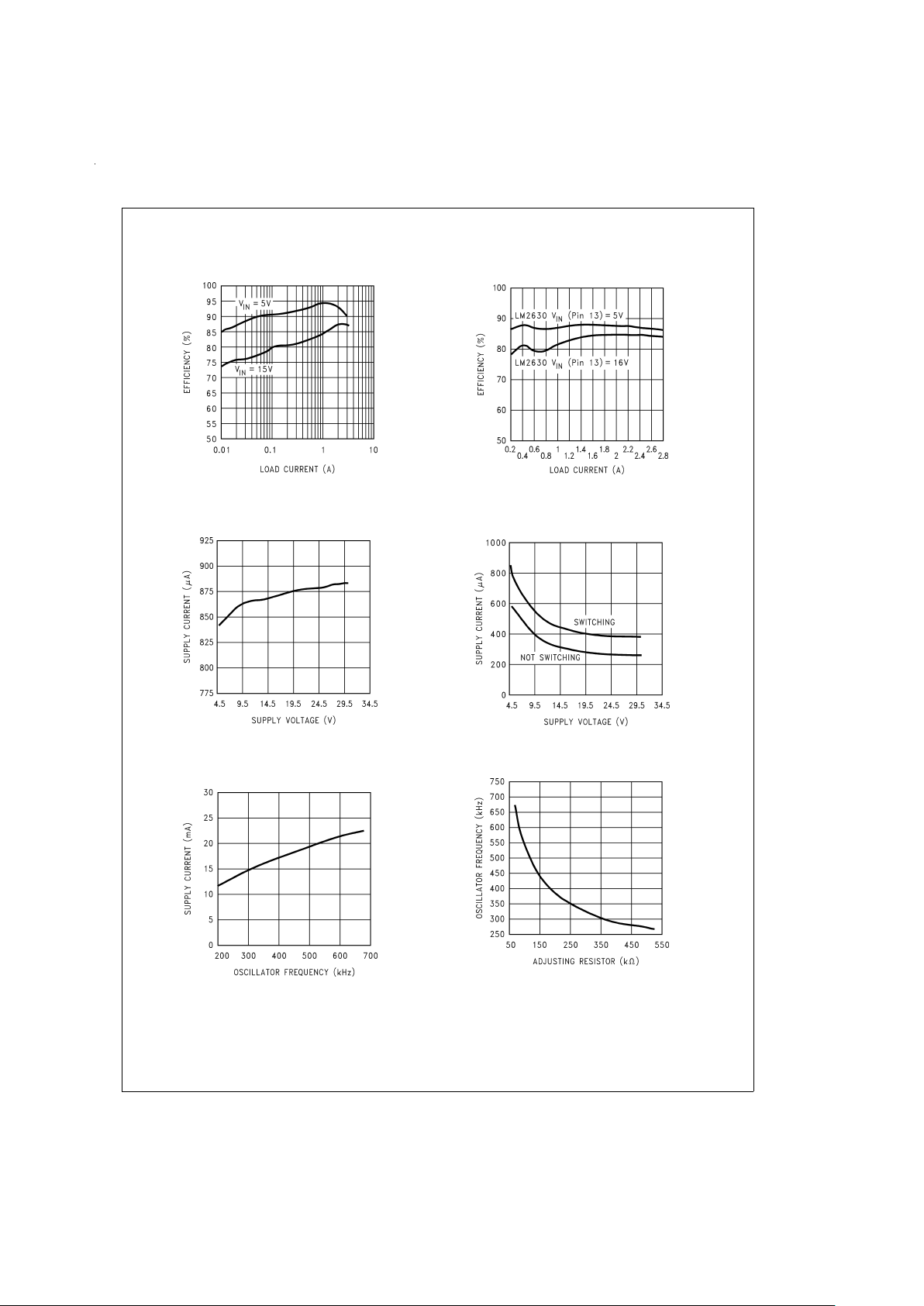
Typical Performance Characteristics
Efficiency vs Load Current
(FPWM=Low, V
OUT
=
3.3V)
DS100120-11
Efficiency (FPWM=High, Input Voltage=16V,
V
OUT
=
2.9V)
DS100120-12
Quiscent Supply Current vs Supply Voltage
(Not Switching, FPWM=Low, V
OUT
=
2.0V)
DS100120-15
Quiscent Supply Current vs Supply Voltage
(FPWM=Low, V
OUT
=
3.3V)
DS100120-16
Supply Current vs Oscillator Frequency
(FPWM=High)
DS100120-17
Oscillator Frequency vs Adjusting Resistor
DS100120-18
www.national.com5
 Loading...