NSC LM2623AMM, LM2623AMDC, LM2623ALDX, LM2623MMX, LM2623LDX Datasheet
...
LM2623
General Purpose, Gated Oscillator Based, DC/DC Boost
Converter
General Description
The LM2623 is a high efficiency, general purpose, step-up
DC-DC switching regulator for battery-powered and low input voltage systems. It accepts an input voltage between .8
and 14 volts and converts it into a regulated output voltage
between 1.24 and 14 volts. Efficiencies up to 90% are
achievable with the LM2623.
In order to adapt to a number of applications, the LM2623
allows the designer to vary the output voltage, the operating
frequency (300kHz to 2 MHz) and duty cycle (17% to 90%)
to optimize the part’s performance. The selected values can
be fixed or can vary with battery voltage or input to output
voltage ratio. The LM2623 uses a very simple, on/off regulation mode to produce good efficiency and stable operation
over a wide operating range. It normally regulates by skipping switching cycles when it reaches the regulation limit
(Pulse Frequency Modulation).
Note: Please read the "Non-Linear Effect" and "Choosing
The Correct C3 Capacitor" sub-sections of the Design Procedure section of this data sheet, so that any challenges with
designing with this part can be taken into account before a
board design/layout is finalized.
For Alternative Solutions, See Also: LM2700, LM2622,
LM2731, LM2733, and LM2621.
Features
n Good Efficiency Over a Very Wide Load Range
n Very Low Output Voltage Ripple
n Small, Mini-SO-8 Package (Half the Footprint of
Standard 8 pin SO Package)
n 1.09 mm Package Height
n Up to 2 MHz Switching Frequency
n .8V to 14V Operating Voltage
n 1.1V Start-up Voltage
n 1.24V - 14V Adjustable Output Voltage
n Up to 2A Load Current at low Output Voltages
n 0.17Ω Internal MOSFET
n Up to 90% Regulator Efficiency
n 80 µA Typical Operating Current (into V
DD
pin of supply)
n
<
2.5µA Guaranteed Supply Current In Shutdown
n 4mm x 4mm Thermally Enhanced LLP Package Option
Applications
n Cameras, Pagers and Cell Phones
n PDAs,Palmtop Computers, GPS devices
n White LED Drive, TFT or Scanned LCDs
n Flash Memory Programming
n Hand-Held Instruments
n 1, 2, 3 or 4 Cell Alkaline Systems
n 1, 2 or 3 Cell Lithium-ion Systems
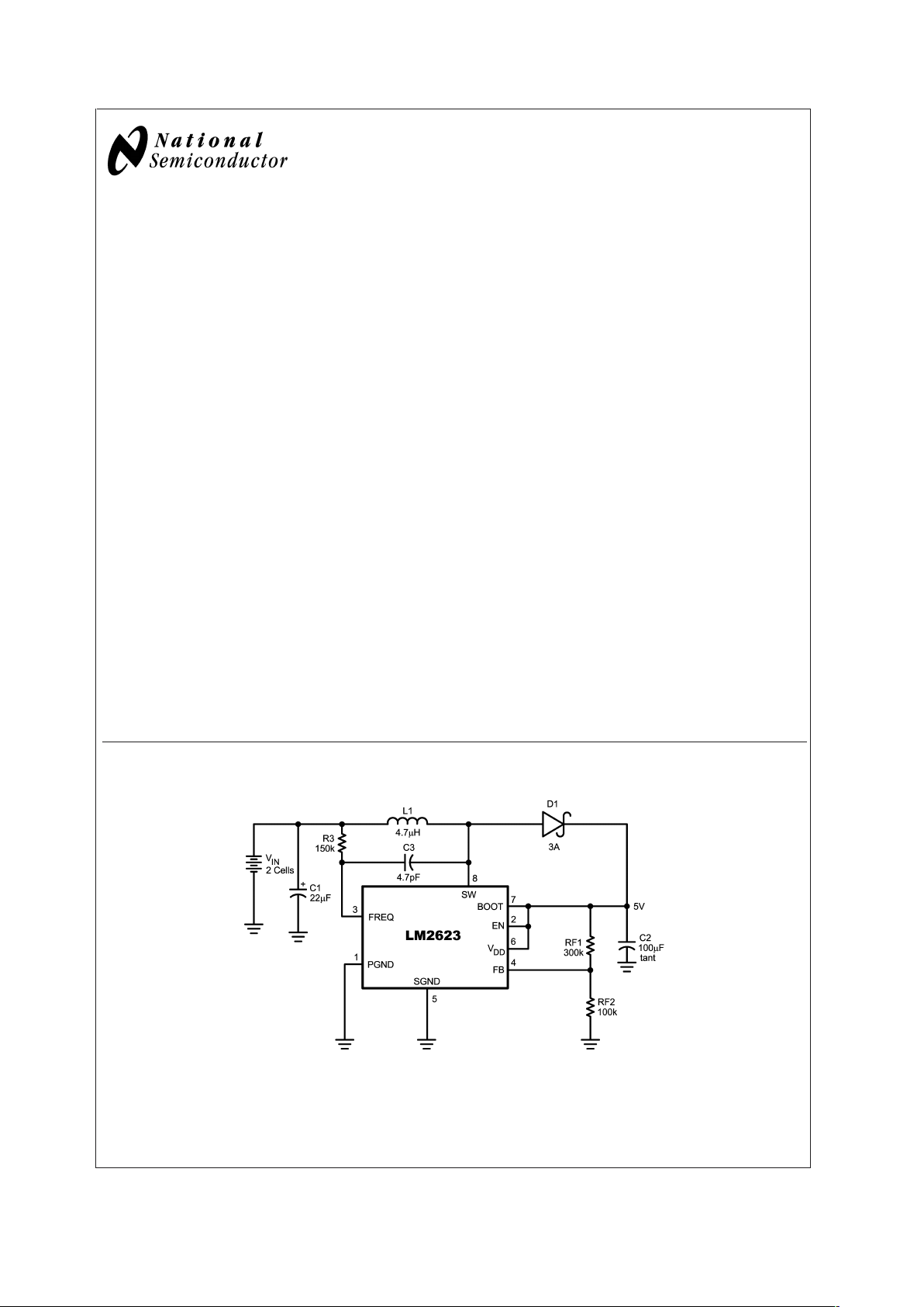
Typical Application Circuit
20038801
July 2003
LM2623 General Purpose, Gated Oscillator Based, DC/DC Boost Converter
© 2003 National Semiconductor Corporation DS200388 www.national.com

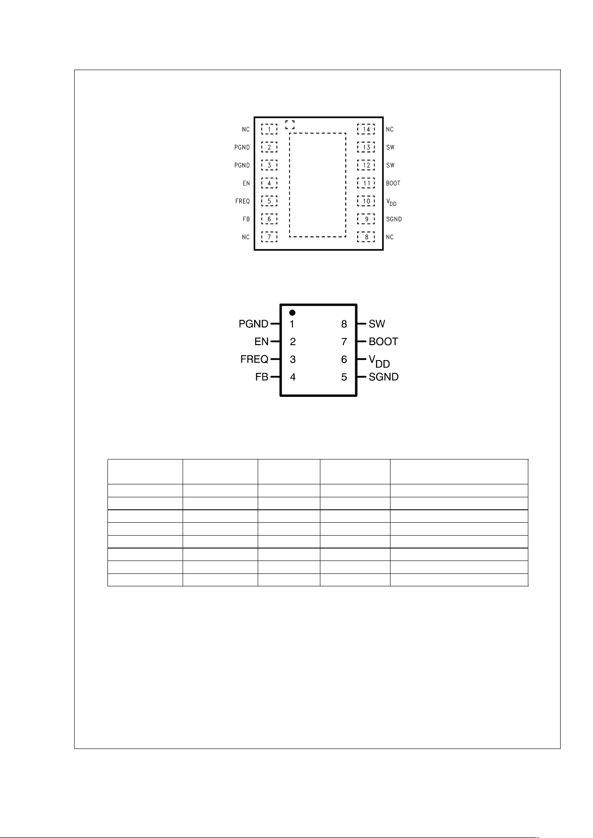
Connection Diagram
LLP Package
20038802
Top View
Mini SO-8 (MM) Package
20038818
Top View
Ordering Information
Order Number Package Type
NSC Package
Drawing
Package
Marking
Supplied As
LM2623MMX Mini SO-8 MUA08A S46B 3000 Units on Tape and Reel
LM2623AMMX Mini SO-8 MUA08A S46A 3000 Units on Tape and Reel
LM2623AMM Mini SO-8 MUA08A S46A 1000 Units on Tape and Reel
LM2623MM Mini SO-8 MUA08A S46B 1000 Units on Tape and Reel
LM2623LDX LLP-14 LDA14A 2623AB 4500 Units on Tape and Reel
LM2623ALDX LLP-14 LDA14A 2623A 4500 Units on Tape and Reel
LM2623LD LLP-14 LDA14A 2623AB 1000 Units on Tape and Reel
LM2623ALD LLP-14 LDA14A 2623A 1000 Units on Tape and Reel
LM2623
www.national.com 2

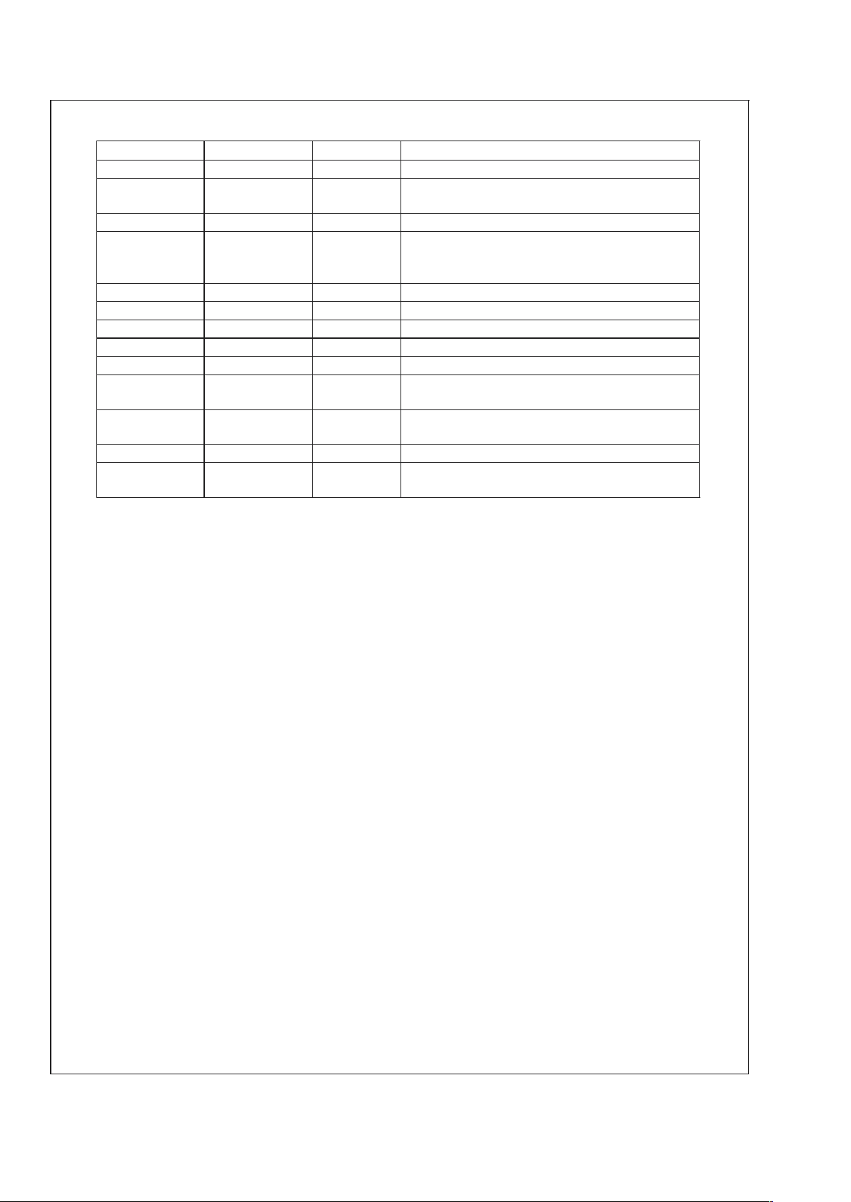
Pin Description
LLP-14 Pin MSOP-8 Pin Name Function
1 NC No Connect
2, 3 1 PGND
Power Ground (LLP Pins2&3must be shorted
together).
4 2 EN Active-Low Shutdown Input
5 3 FREQ Frequency Adjust. An external resistor connected
between this pin and a voltage source sets the
switching frequency of the LM2623.
6 4 FB Output Voltage Feedback
7 NC No Connect
8 NC No connect
9 5 SGND Signal Ground
10 6 V
DD
Power Supply for Internal Circuitry
11 7 BOOT
Bootstrap Supply for the Gate Drive of Internal
MOSFET Power Switch
12, 13 8 SW
Drain of the Internal MOSFET Power Switch. (LLP Pins
12&13must be shorted together).
14 NC No Connect
DAP DAP
To be soldered to board for enhanced thermal
dissipation. To be electrically isolated/floating.
LM2623
www.national.com3

Absolute Maximum Ratings (Note 1)
If Military/Aerospace specified devices are required,
please contact the National Semiconductor Sales Office/
Distributors for availability and specifications.
SW Pin Voltage −0.5 V to 14.5V
BOOT, V
DD
, EN and FB Pins −0.5V to 10V
FREQ Pin 100µA
T
Jmax
(Note 2) 150˚C
Storage Temperature Range −65˚C to +150˚C
Lead Temp. (Soldering, 5 sec) 260˚C
Power Dissipation (T
A
=25˚C)
(Note 2)
500mW
ESD Rating (Note 3) 2kV
Operating Conditions (Note 1)
V
DD
Pin 3V to 5V
FB, EN Pins 0 to V
DD
BOOT Pin 0 to 10V
Ambient Temperature (T
A
) −40˚C to +85˚C
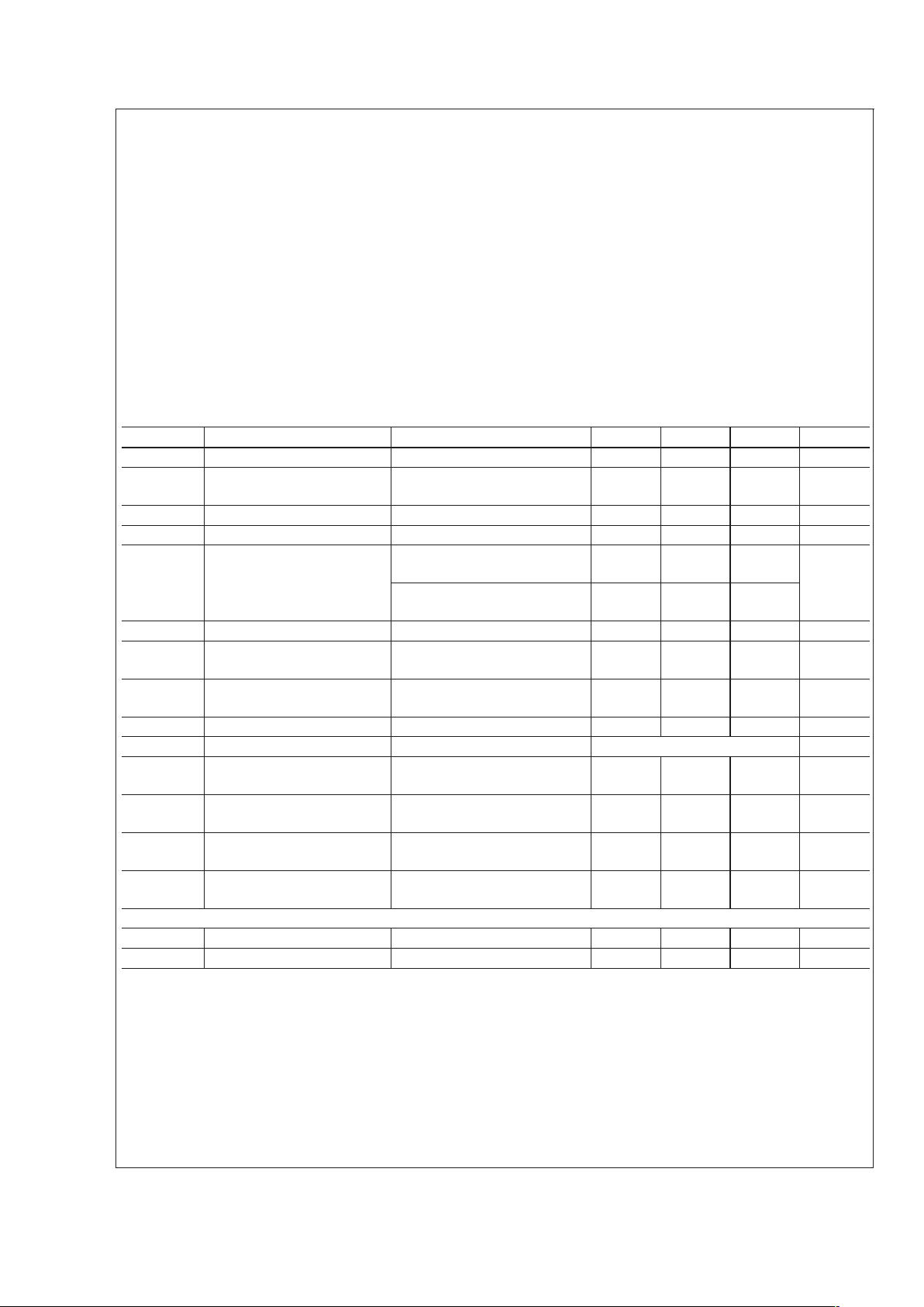
Electrical Characteristics
Limits in standard typeface are for TJ= 25˚C, and limits in boldface type apply over the full operating temperature range of
−40˚C to +85˚C. Unless otherwise specified: V
DD=VOUT
= 3.3V.
Symbol Parameter Condition Typ Min Max Units
V
DD_ST
Start-Up Supply Voltage 25˚C I
LOAD
= 0mA (Note 4) 1.1 V
V
IN_OP
Minimum Operating Supply
Voltage (once started)
I
LOAD
= 0mA 0.65 .8 V
V
FB
FB Pin Voltage 1.24 1.2028 1.2772 V
V
OUT_MAX
Maximum Output Voltage 14 V
η Efficiency V
IN
= 3.6V; V
OUT
= 5V; I
LOAD
=
500mA
87
%
V
IN
= 2.5V; V
OUT
= 3.3V; I
LOAD
= 200mA
87
D Switch Duty Cycle 17 %
I
DD
Operating Quiescent Current
(Note 5)
FB Pin>1.3V; EN Pin at V
DD
80 110 µA
I
SD
Shutdown Quiescent Current
(Note 6)
VDD, BOOT and SW Pins at
5.0V; EN Pin
<
200mV
0.01 2.5 µA
I
CL
Switch Peak Current Limit LM2623A 2. 85 2.2 A
I
C
Switch Peak Current Limit LM2623 1.2 A
R
DS_ON
MOSFET Switch On
Resistance
0.17 0.26 Ω
θ
JA
Thermal Resistance MM Package, Junction to
Ambient(Note 2)
240 ˚C/W
θ
JA
Thermal Resistance LLP Package, Junction to
Ambient(Notes 2, 8)
40 ˚C/W
θ
JA
Thermal Resistance LLP Package, Junction to
Ambient(Notes 2, 9)
56 ˚C/W
Enable Section
V
EN_LO
EN Pin Voltage Low (Note 7) 0.15V
DD
V
V
EN_HI
EN Pin Voltage High (Note 7) 0.7V
DD
V
Note 1: Absolute maximum ratings indicate limits beyond which damage to the device may occur. Electrical specifications do not apply when operating the device
outside of its rated operating conditions.
Note 2: The maximum power dissipation must be derated at elevated temperatures and is dictated by T
jmax
(maximum junction temperature), θJA(junction to
ambient thermal resistance), and T
A
(ambient temperature). The maximum allowable power dissipation at any temperature is P
dmax
=(T
jmax-TA
)/ θJAor the number
given in the Absolute Maximum Ratings, whichever is lower.
Note 3: The human body model is a 100 pF capacitor discharged through a 1.5 kΩ resistor into each pin. For Pin 8 (SW) the ESD rating is 1.0 kV.
Note 4: V
DD
tied to Boot and EN pins. Frequency pin tied to VDDthrough 121K resistor. V
DD_ST=VDD
when startu-up occurs. VINis VDD+ D1 voltage (usually
10-50 mv at start-up)
Note 5: This is the current into the V
DD
pin.
Note 6: This is the total current into pins V
DD
, BOOT, SW and FREQ.
Note 7: When the EN pin is below V
EN_LO
, the regulator is shut down; when it is above V
EN_HI
, the regulator is operating.
LM2623
www.national.com 4
 Loading...