

NSC LM2619ATLX, LM2619ATL Datasheet

November 2002
LM2619
500mA Sub-Miniature Step-Down DC-DC Converter
LM2619 500mA Sub-Miniature Step-Down DC-DC Converter
General Description
The LM2619 step down DC-DC converter is optimized for
powering circuits from a single Lithium-Ion cell. It steps down
an input voltage of 2.8V to 5.5V to an output of 1.5V to 3.6V
at up to 500mA. Output voltage is set using resistor feedback
dividers.
The device offers three modes for mobile phones and similar
portable applications. Fixed-frequency PWM mode minimizes RF interference. A SYNC input allows synchronizing
the switching frequency in a range of 500kHz to 1MHz. Low
current hysteretic PFM mode reduces quiescent current to
160µA (typ.). Shutdown mode turns the device off and reduces battery consumption to 0.02µA (typ.).
Current limit and thermal shutdown features protect the device and system during fault conditions.
The LM2619 is available in a 10 bump micro SMD package.
This packaging uses National’s chip-scale micro SMD technology and offers the smallest possible size. A high switching
frequency (600kHz) allows use of tiny surface-mount components.
The device features external compensation to tailor the response to a wide range of operating conditions.
Key Specifications
n Operates from a single LiION cell (2.8V to 5.5V)
n Output voltage (1.5V to 3.6V)
±
n
1% DC feedback voltage precision
n 500mA maximum load capability
n 600µA typ PWM mode quiescent current
n 0.02µA typ shutdown current
n 600kHz PWM switching frequency
n SYNC input for PWM mode frequency synchronization
from 500kHz to 1MHz
n High efficiency (96% typ at 3.9V
in PWM mode from internal synchronous rectification
n 100% Maximum Duty Cycle for Lowest Dropout
, 3.6V
IN
and 200mA)
OUT
Features
n Sub-miniature 10-bump thin micro SMD package
n Uses small ceramic capacitors
n 5mV typ PWM mode output voltage ripple(C
n Internal soft start
n Current overload protection
n Thermal Shutdown
n External compensation
OUT
= 22µF)
Applications
n Mobile Phones
n Hand-Held Radios
n RF PC Cards
n Wireless LAN Cards
© 2002 National Semiconductor Corporation DS200574 www.national.com
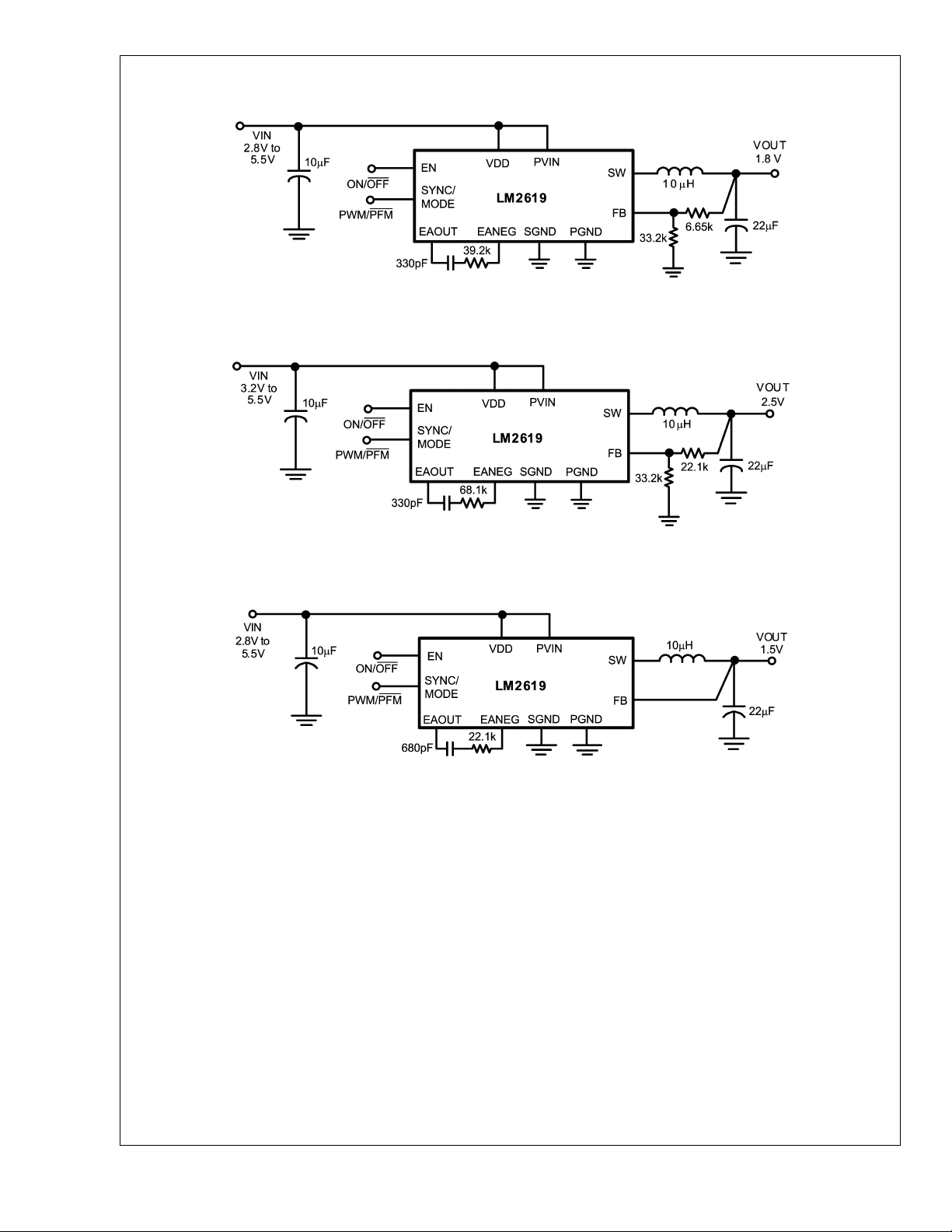
Typical Application Circuits
LM2619
20057401
FIGURE 1. Typical Circuit for 1.8V Output Voltage
FIGURE 2. Typical Circuit for 2.5V Output Voltage
FIGURE 3. Typical Circuit for 1.5V Output Voltage
20057402
20057403
www.national.com 2
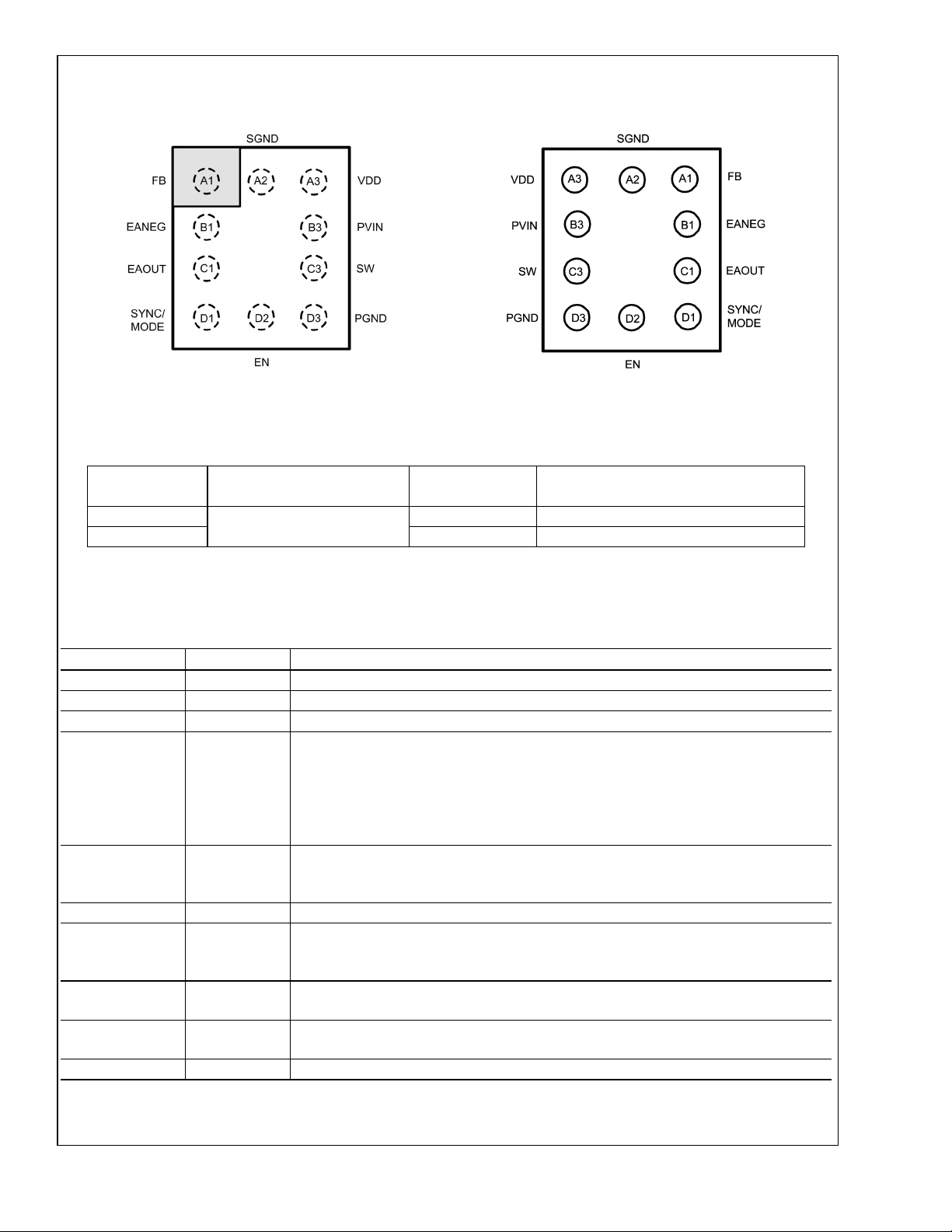
Connection Diagrams
10-Bump micro SMD Package
LM2619
Top View
20057404
Bottom View
20057405
Ordering Information
Order Number Package Type
LM2619ATL
LM2619ATLX XYTT S76A 3000 Tape and Reel
(*) XY - denotes the date code marking (2 digit) in production
(*) TT - refers to die run/lot traceability for production
(*) S - product line designator
Package markings may change over the course of production.
10-bump Wafer Level Chip Scale
(micro SMD)
NSC Package
*
Marking (
XYTT S76A 250 Tape and Reel
)
Supplied As
Pin Description
Pin Number Pin Name Function
A1 FB Feedback Analog Input.
B1 EANEG Inverting input of error amplifier.
C1 EAOUT Output of error amplifier.
D1 SYNC/MODE Synchronization Input. Use this digital input for frequency selection or modulation control.
Set:
SYNC/MODE = high for low-noise 600kHz PWM mode
SYNC/MODE = low for low-current PFM mode
SYNC/MODE = a 500kHz– 1MHz external clock for synchronization in PWM mode. (See
Synchronization and Operating Modes in the Device Information section.)
D2 EN Enable Input. Set this Schmitt trigger digital input high for normal operation. For shutdown,
set low. Set EN low during system power-up and other low supply voltage conditions.
(See Shutdown Mode in the Device Information section.)
D3 PGND Power Ground.
C3 SW Switching Node connection to the internal PFET switch and NFET synchronous rectifier.
Connect to an inductor with a saturation current rating that exceeds the max Switch Peak
Current Limit of the LM2619.
B3 PVIN Power Supply Voltage Input to the internal PFET switch. Connect to the input filter
capacitor.
A3 VDD Analog Supply Input. If board layout is not optimum, an optional 0.1µF ceramic capacitor
is suggested.
A2 SGND Analog and Control Ground.
www.national.com3
Absolute Maximum Ratings (Note 1)
If Military/Aerospace specified devices are required,
LM2619
please contact the National Semiconductor Sales Office/
Distributors for availability and specifications.
PVIN, VDD to SGND −0.2V to +6V
PGND to SGND, PVIN to VDD −0.2V to +0.2V
EN, EAOUT, EANEG, SYNC/MODE
Storage Temperature Range −45˚C to +150˚C
Lead Temperature
(Soldering, 10 sec.) 260˚C
Junction Temperature (Note 2) −25˚C to +125˚C
Minimum ESD Rating
(Human Body Model, C = 100 pF, R = 1.5 kΩ)
Thermal Resistance (θ
) (Note 3) 140˚C/W
JA
to SGND −0.2V to +6V
FB, SW (GND −0.2V) to
(VDD +0.2V)
Electrical Characteristics
Specifications with standard typeface are for TA=TJ= 25˚C, and those in boldface type apply over the full Operating Temperature Range of T
Symbol Parameter Conditions Min Typ Max Units
V
V
V
IN
FB
HYST
Input Voltage Range PVIN = VDD = VIN(Note 4) 2.8 3.6 5.5 V
Feedback Voltage 1.485 1.50 1.515 V
PFM Comparator Hysteresis
Voltage
I
SHDN
I
Q1_PWM
I
Q2_PFM
R
DSON (P)
Shutdown Supply Current VIN = 3.6V, EN = 0V 0.02 3 µA
DC Bias Current into VDD SYNC/MODE = VIN
Pin-Pin Resistance for
P FET
R
DSON (N)
Pin-Pin Resistance for
N FET
R
DSON (TC)
FET Resistance
Temperature Coefficient
I
LIM
Switch Peak Current Limit
(Note 6)
V
IH
Logic High Input, EN,
SYNC/MODE
V
IL
Logic Low Input, EN,
SYNC/MODE
F
SYNC
SYNC/MODE Clock
Frequency Range
F
OSC
Internal Oscillator
Frequency
T
min
Minimum ON-Time of PFET
Switch in PWM Mode
Note 1: Absolute Maximum Ratings indicate limits beyond which damage to the device may occur. Operating Ratings indicate conditions for which the device is
functional, but device specifications may not be guaranteed. For guaranteed specifications and associated test conditions, see the Min and Max limits and Conditions
in the Electrical Characteristics table. Typical (typ) specifications are mean or average values at 25˚C and are not guaranteed.
Note 2: Thermal shutdown will occur if the junction temperature exceeds 150˚C.
Note 3: Thermal resistance specified with 2 layer PCB (0.5/0.5 oz. cu).
Note 4: The LM2619 is designed for mobile phone applications where turn-on after system power-up is controlled by the system controller. Thus, it should be kept
in shutdown by holding the EN pin low until the input voltage exceeds 2.8V.
Note 5: The hysteresis voltage is the minimum voltage swing on the FB pin that causes the internal feedback and control circuitry to turn the internal PFET switch
on and then off during PFM mode. When resistor dividers are used like in the operating circuit of Figure 4, the hysteresis at the output will be the value of the
hysteresis at the feedback pin times the resistor divider ratio. In this case, 24mV (typ) x ((46.4k + 33.2k)/33.2k).
Note 6: Current limit is built-in, fixed, and not adjustable. If the current limit is reached while the voltage at the FB pin is pulled below 0.7V, the internal PFET switch
turns off for 2.5µs to allow the inductor current to diminish.
Note 7: SYNC driven with an external clock switching between V
the external clock frequency. The LM2619 synchronizes to the rising edge of the external clock.
= −25˚C to +85˚C. Unless otherwise specified, PVIN = VDD = EN = SYNC/MODE = 3.6V.
A=TJ
PFM Mode (SYNC/MODE =
0V) (Note 5)
FB=2V
SYNC/MODE = 0V
FB=2V
24 mV
600 725 µA
160 195 µA
395 550 mΩ
330 500 mΩ
0.5 %/C
620 810 1000 mA
0.95 1.3 V
0.4 0.80 V
(Note 7)
PWM Mode
500 1000 kHz
468 600 732 kHz
200 ns
and GND. When an external clock is present at SYNC; the IC is forced to be in PWM mode at
IN
±
2kV
www.national.com 4
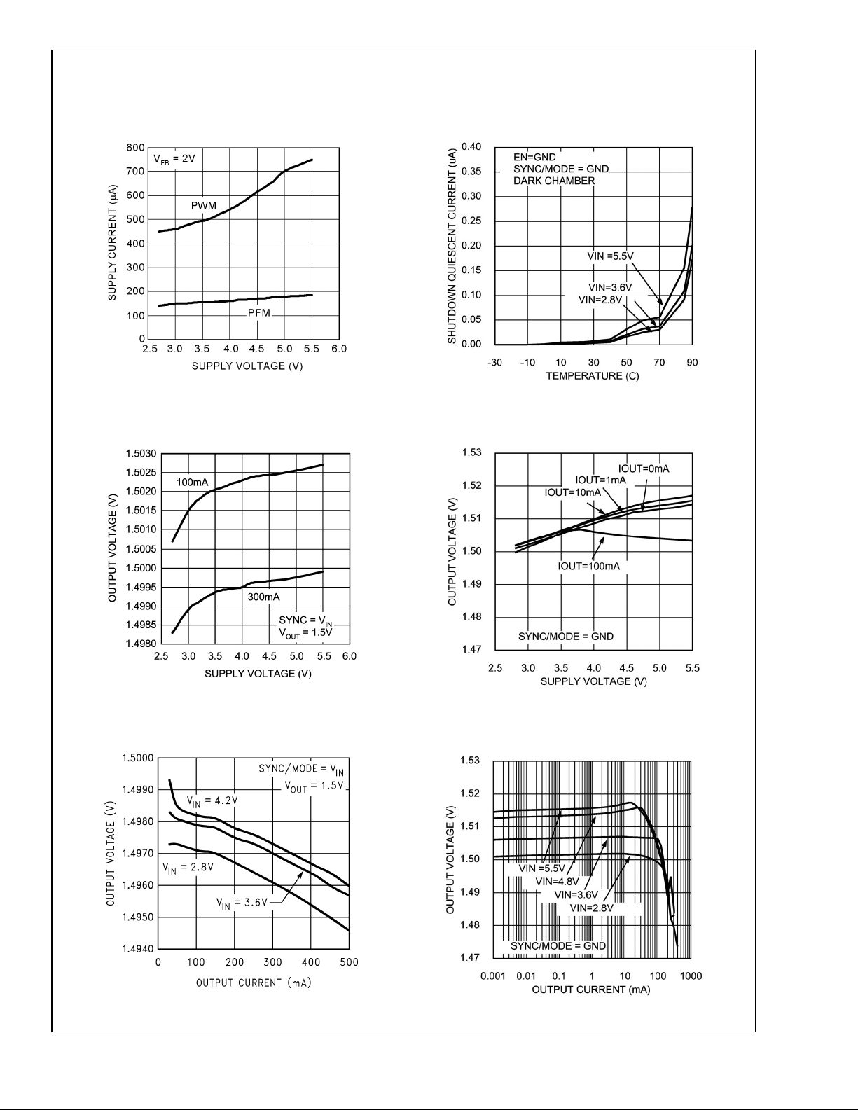
LM2619
Typical Performance Characteristics LM2619ATL, Circuit of Figure 3,V
less otherwise noted.
Shutdown Quiescent Current vs Temperature
Quiescent Supply Current vs Supply Voltage
20057408
Output Voltage vs Supply Voltage
= 1.5V, PWM MODE)
(V
OUT
(Circuit in Figure 3)
Output Voltage vs Supply Voltage
(V
= 1.5V, PFM MODE)
OUT
= 3.6V, TA= 25˚C, un-
IN
20057422
Output Voltage vs Output Current
= 1.5V, PWM MODE)
(V
OUT
20057409
20057411
Output Voltage vs Output Current
(V
= 1.5V, PFM MODE)
OUT
20057410
20057413
www.national.com5
 Loading...