

NSC LM2612BBPX, LM2612ABPX, LM2612ABP, LM2612BBP Datasheet
May 2002
LM2612
400mA Sub-miniature, Programmable, Step-Down DC-DC
Converter for Ultra Low-Voltage Circuits
LM2612 400mA Sub-miniature, Programmable, Step-Down DC-DC Converter for Ultra Low-Voltage
Circuits
General Description
The LM2612 step-down DC-DC converter is optimized for
powering ultra-low voltage circuits from a single Lithium-Ion
cell. It provides up to 400mA (300mA for B grade), over an
input voltage range of 2.8V to 5.5V. Pin programmable output voltages of 1.05V, 1.3V, 1.5V or 1.8V allow adjustment
for MPU voltage options without board redesign or external
feedback resistors.
The device has three pin-selectable modes for maximizing
battery life in mobile phones and similar portable applications. Low-noise PWM mode offers 600kHz fixed-frequency
operation to reduce interference in RF and data acquisition
applications during full-power operation. In PWM mode, internal synchronous rectification provides high efficiency
(91% typ. at 1.8V
the switching frequency in a range of 500kHz to 1MHz to
avoid noise from intermodulation with system frequencies.
Low-current hysteretic PFM mode reduces quiescent current
to 150 µA (typ.) during system standby. Shutdown mode
turns the device off and reduces battery consumption to
0.1µA(typ.).Additional features include soft start and current
overload protection.
The LM2612 is available in a 10 pin micro SMD packge. This
package uses National’s wafer level chip-scale micro SMD
technology and offers the smallest possible size. Only three
small external surface-mount components, an inductor and
two ceramic capacitors are required.
). A SYNC input allows synchronizing
OUT
Key Specifications
n Operates from a single LiION cell (2.8V to 5.5V)
n Pin programmable output voltage (1.05V, 1.3V, 1.5V and
1.8V)
n 400mA maximum load capability (300mA for B grade)
±
n
2% PWM mode DC output voltage precision
n 2mV typ PWM mode output voltage ripple
n 150 µA typ PFM mode quiescent current
n 0.1µA typ shutdown mode current
n Internal synchronous rectification for high PWM mode
efficiency (91% at 2.8V
n 600kHz PWM mode switching frequency
n SYNC input for PWM mode frequency synchronization
from 500kHz to 1MHz
, 1.8V
IN
OUT
)
Features
n Sub-miniature 10-pin micro SMD package
n Only three tiny surface-mount external components
required
n Uses small ceramic capacitors.
n Internal soft start
n Current overload protection
n No external compensation required
Applications
n Mobile Phones
n Hand-Held Radios
n Battery Powered Devices
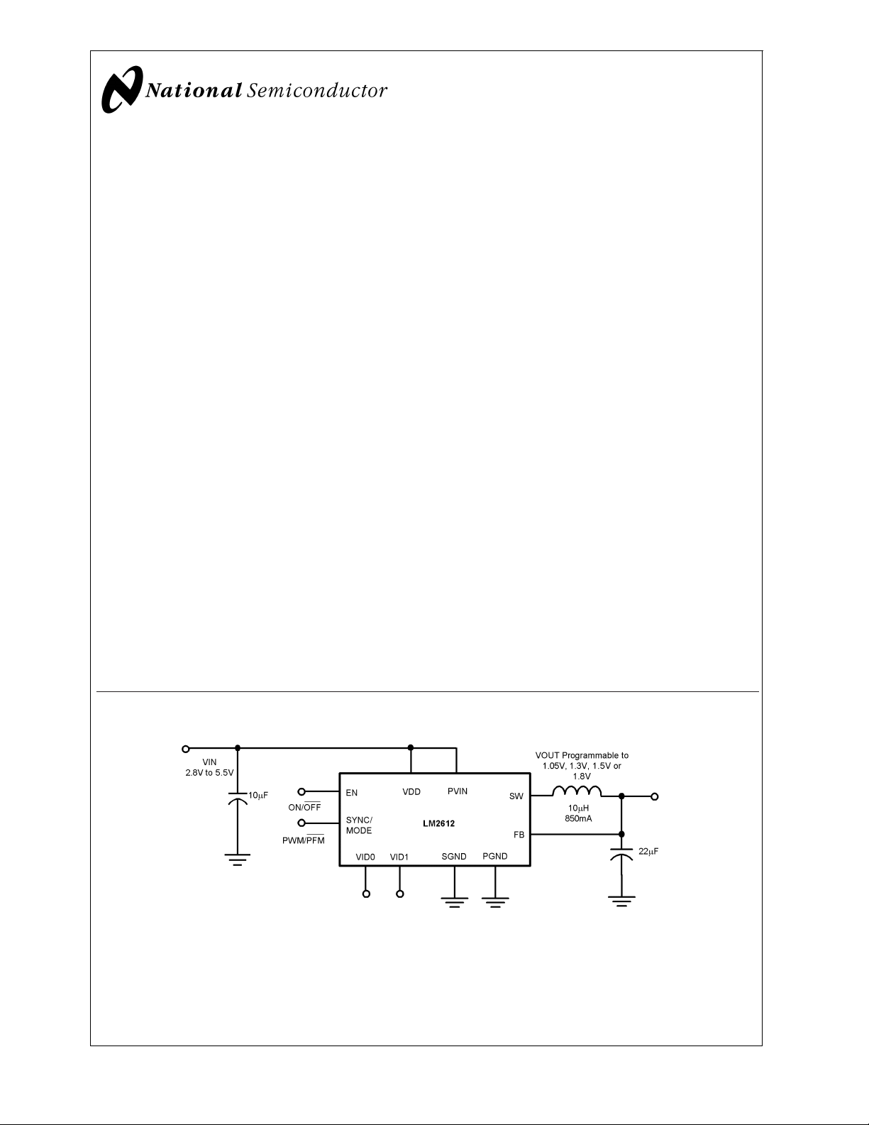
Typical Application Circuit
20007102
© 2002 National Semiconductor Corporation DS200071 www.national.com

Connection Diagrams
LM2612
micro SMD package
TOP VIEW
20007104
BOTTOM VIEW
20007105
Ordering Information
Order Number Package Type NSC Package
Drawing
10-Pin micro SMD
LM2612ABP
LM2612BBP 250 Units, Tape and Reel
LM2612ABPX 3000 Units, Tape and Reel
LM2612BBPX 3000 Units, Tape and Reel
10-bump Wafer Level Chip Scale
(micro SMD)
BPA10VWB
250 Units, Tape and Reel
Supplied As
Pin Description
Pin Number(*) Pin Name Function
A1 FB Feedback Analog Input. Connect to the output at the output filter capacitor (Figure 1)
B1 VID1 Output Voltage Control Inputs. Set the output voltage using these digital inputs (see Table
C1 VID0
D1 SYNC/MODE Synchronization Input. Use this digital input for frequency selection or modulation control.
D2 EN Enable Input. Set this CMOS Schmitt trigger digital input high to VDD for normal
D3 PGND Power Ground
C3 SW Switching Node connection to the internal PFET switch and NFET synchronous rectifier.
B3 PVIN Power Supply Input to the internal PFET switch. Connect to the input filter capacitor
A3 VDD Analog Supply Input. If board layout is not optimum, an optional 0.1µF ceramic capacitor
A2 SGND Analog and Control Ground
(*) note the pin numbering scheme for the MicroSMD package was revised in April, 2002 to comform to JEDEC standard. Only the pin numbers were revised. No
changes to the physical location of the inputs/outputs were made. For reference purpose, the obsolete numbering has FB as pin 1, VID1 as pin 2, VID0 as pin3,
SYNC as pin 4, EN as pin 5, PGND as pin 6, SW as pin 7, PVIN as pin 8, VDD as pin 9 and SGND as pin 10.
1). The output defaults to 1.5V if these pins are unconnected.
Set:
SYNC/MODE = high for low-noise 600kHz PWM mode
SYNC/MODE = low for low-current PFM mode
SYNC/MODE = a 500kHz - 1MHz external clock for synchronization to an external clock in
PWM mode. See
operation. For shutdown, set low to SGND. Set EN low during power-up and other low
supply voltage conditions. (See
Connect to an inductor with a saturation current rating that exceeds the 850mA max
Switch Peak Current Limit specification of the LM2612 (
(
Figure 1
is suggested (
).
Synchronization and Operating Modes
Shutdown Mode
Figure 1
)
in the
in the
Device Information
Figure 1
Device Information
section.)
)
section.
www.national.com 2

LM2612
Absolute Maximum Ratings (Note 1)
If Military/Aerospace specified devices are required,
please contact the National Semiconductor Sales Office/
Distributors for availability and specifications.
PVIN, VDD, to SGND −0.2V to +6V
PGND to SGND −0.2V to +0.2V
EN, SYNC/MODE, VID0, VID1 to
SGND −0.2V to +6V
Lead temperature
(Soldering, 10 sec.) 260˚C
Junction Temperature (Note 2) −25˚C to 125˚C
Minimum ESD Rating
Human body model, C = 100pF, R =
1.5 kΩ
Thermal Resistance (θ
)
JA
±
2.5kV
LM2612ABP & LM2612BBP (Note 3) 170˚C/W
FB, SW (GND −0.2V) to
(VDD +0.2V)
Storage Temperature Range −45˚C to +150˚C
Electrical Characteristics
Specifications with standard typeface are for TA=TJ= 25˚C, and those in bold face type apply over the full Operating Temperature Range (T
0V.
Symbol Parameter Conditions Min Typ Max Units
V
V
V
IN
FB
HYST
Input Voltage Range (Note5)PVIN = VDD = VID1 = VIN,
Feedback Voltage
(Note 6)
PFM Comparator Hysteresis
Voltage
(Note 7)
I
SHDN
I
Q1
I
Q2
R
DSON (P)
Shutdown Supply Current EN = 0V 0.1 3 µA
DC Bias Current into VDD
(V
OUT
Pin-Pin Resistance for P
FET
R
DSON (N)
Pin-Pin Resistance for N
FET
R
DSON , TC
FET Resistance
Temperature Coefficient
I
lim
Switch Peak Current Limit
(Note 8)
V
EN_H
EN Positive Going
Threshold Voltage
(Note 8)
V
EN_L
EN Negative Going
Threshold Voltage
(Note 8)
V
SYNC_H
SYNC/MODE Positive
Going Threshold Voltage
V
SYNC_L
SYNC/MODE Negative
Going Threshold Voltage
V
ID_H
V
ID0,VID1
Threshold Voltage
V
ID_L
V
ID0,VID1
Threshold Voltage
= −25˚C to +85˚C). Unless otherwise specified, PVIN = VDD = EN = SYNC = 3.6V, VID0 = VID1 =
A=TJ
VID0 = 0V
VID0 = V
VID0 = V
, VID1 = V
IN
, VID1 = 0V 1.274 1.30 1.326
IN
IN
2.8 5.5 V
1.00 1.05 1.10
VID0 = 0V, VID1 = 0V 1.470 1.50 1.530
VID0 = 0V, VID1 = V
IN
1.764 1.8 1.836
PFM Mode (SYNC = 0V)
16 mV
set to 1.5V)
No-Load, PFM mode
(SYNC/MODE = 0V)
No-Load, PWM mode
(SYNC/MODE = V
)
IN
LM2612ABP & LM2612BBP
LM2612ABP & LM2612BBP
150 185
555 725
370 500 mΩ
330 500 mΩ
0.5 %/C
LM2612ABP 510 690 850
LM2612BBP 400 690 980
= 3.6V
V
DD
2.54 2.85 V
= 3.6V
V
DD
1.70 2.00 V
0.95 1.3 V
0.4 0.9 V
Positive Going
Negative Going
0.4 0.83 V
0.92 1.2 V
V
µA
mA
www.national.com3

Electrical Characteristics (Continued)
Specifications with standard typeface are for TA=TJ= 25˚C, and those in bold face type apply over the full Operating Tem-
LM2612
perature Range (T
0V.
Symbol Parameter Conditions Min Typ Max Units
I
VID
VID1, VID0 Pull Down
Current
f
sync
SYNC/MODE Clock
Frequency Range
(Note 10)
F
OSC
Internal Oscillator
Frequency
T
min
Minimum ON-Time of P FET
Switch in PWM Mode
Load Transient Response in
PWM Mode
Line Transient Response in
PFM Mode
Note 1: Absolute Maximum Ratings indicate limits beyond which damage to the device may occur. Operating Ratings are conditions for which the device is intended
to be functional, but parameter specifications may not be guaranteed. For guaranteed specifications and associated test conditions, see the Min and Max limits and
Conditions in the Electrical Characteristics table. Electrical Characteristics table limits are guaranteed by production testing, design or correlation using standard
Statistical Quality Control methods. Typical (Typ) specifications are mean or average values from characterization at 25C and are not guaranteed.
Note 2: In PWM mode, Thermal shutdown will occur if the junction temperature exceeds the 150˚C maximum junction temperature of the device.
Note 3: Thermal resistance specified with 2 layer PCB(0.5/0.5 oz. cu).
Note 4: Thermal resistance specified with 3 layer PCB (2/1/1 oz. cu) and 12 vias 0.33mm diameter (see Application Note AN-1187).
Note 5: The LM2612 is designed for cell phone applications where turn-on after power-up is controlled by the system processor and internal UVLO (Under Voltage
LockOut) circuitry is unecessary. The LM2612 has no UVLO circuitry and should be kept in shutdown by holding the EN pin low until the input voltage exceeds 2.8V.
Although the LM2612 exhibited safe behavior during pre-production evaluation while enabled at low input voltages, this is not guaranteed.
Note 6: The feedback voltage is trimmed at the 1.5V output setting. The other output voltages result from the pin selection of the internal DAC’s divider ratios. The
precision for the feedback voltages is
if trimming at other voltages is desired.
Note 7: : The hysteresis voltage is the minimum voltage swing on FB that causes the internal feedback and control circuitry to turn the internal PFET switch on and
then off, during PFM mode.
Note 8: Current limit is built-in, fixed, and not adjustable. If the current limit is reached while the output is pulled below about 0.7V, the internal PFET switch turns
off for 2.5 µs to allow the inductor current to diminish.
Note 9: EN is a CMOS Schmitt trigger digital input with logic thresholds that scale with the supply voltage at the VDD pin. The nominal logic thresholds are
approximately 0.71VDD and 0.55VDD for the high and low thresholds respectively.
Note 10: SYNC driven with an external clock switching between V
external clock frequency. The LM2612 synchronizes to the rising edge of the external clock.
= −25˚C to +85˚C). Unless otherwise specified, PVIN = VDD = EN = SYNC = 3.6V, VID0 = VID1 =
A=TJ
VID1, VID0 = 3.6V
1.8 µA
500 1000 kHz
LM2612ABP, PWM Mode
(SYNC = VIN)
LM2612BBP, PWM Mode
(SYNC = VIN)
468 600 732
450 600 750
200 ns
Circuit of
I
OUT
Circuit of
VIN= 3.0V to 3.6V Step
t
r=tp
±
2%, except for the 1.05V setting, which is 5%. Contact the Portable Power Applications group at National Semiconductor,
Figure 1
= 20mA to 200mA Step
±
25 mV
Figure 1
±
3mV
=10µs
and GND. When an external clock is present at SYNC, the IC is forced to PWM mode at the
IN
kHz
www.national.com 4
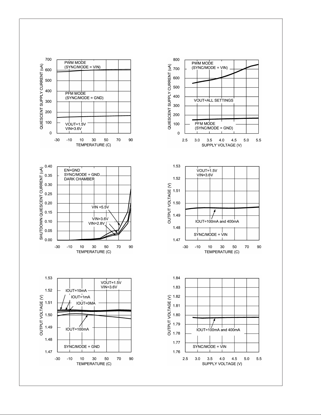
Typical Operating Characteristics
LM2612ABP, Circuit of
L
= 10 µH, unless otherwise noted.
1
Quiescent Supply Current vs Temperature Quiescent Supply Current vs Supply Voltage
Shutdown Quiescent Current vs Temperature Output Voltage vs Temperature (PWM Mode)
Figure 1
,VIN= 3.6V, TA= 25˚C,
20007106 20007107
LM2612
20007108
Output Voltage vs Temperature (PFM Mode)
20007110 20007111
Output Voltage vs Supply Voltage
(V
= 1.8V, PWM Mode)
OUT
20007109
www.national.com5
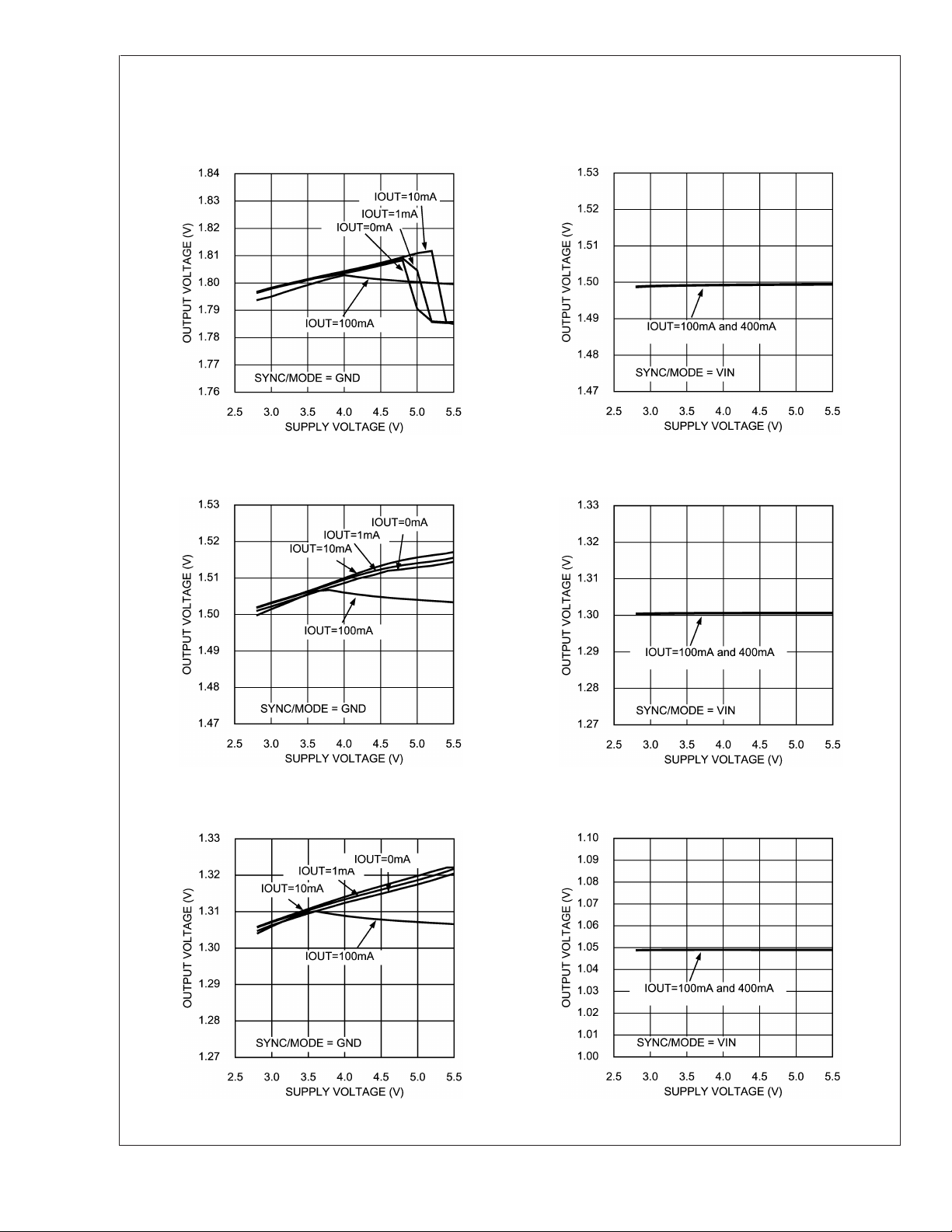
Typical Operating Characteristics LM2612ABP, Circuit of
µH, unless otherwise noted. (Continued)
LM2612
Output Voltage vs Supply Voltage
(V
= 1.8V, PFM Mode)
OUT
20007112 20007113
Output Voltage vs Supply Voltage
(V
= 1.5V, PFM Mode)
OUT
Figure 1
,VIN= 3.6V, TA= 25˚C, L1=10
Output Voltage vs Supply Voltage
(V
= 1.5V, PWM Mode)
OUT
Output Voltage vs Supply Voltage
(V
= 1.3V, PWM Mode)
OUT
20007114
Output Voltage vs Supply Voltage
(V
= 1.3V, PFM Mode)
OUT
20007116 20007117
www.national.com 6
Output Voltage vs Supply Voltage
(V
= 1.05V, PWM Mode)
OUT
20007115
 Loading...