

NSC LM20154MH, LM20154 Datasheet

November 13, 2007
LM20154
4A, 1MHz PowerWise® Synchronous Buck Regulator with
SYNCOUT
General Description
The LM20154 is a full featured 1 MHz synchronous buck regulator capable of delivering up to 4A of continuous output
current. The current mode control loop can be compensated
to be stable with virtually any type of output capacitor. For
most cases, compensating the device only requires two external components, providing maximum flexibility and ease of
use. The device is optimized to work over the input voltage
range of 2.95V to 5.5V making it suited for a wide variety of
low voltage systems.
The device features internal over voltage protection (OVP)
and over current protection (OCP) circuits for increased system reliability. A precision enable pin and integrated UVLO
allows the turn on of the device to be tightly controlled and
sequenced. Start-up inrush currents are limited by both an
internally fixed and externally adjustable Soft-Start circuit.
Fault detection and supply sequencing is possible with the
integrated power good circuit.
The LM20154 features an open drain SYNCOUT pin which
provides an external clock that matches the switching frequency of the device but is shifted by 180 degrees.
The LM20154 is designed to work well in multi-rail power
supply architectures. The output voltage of the device can be
configured to track a higher voltage rail using the SS/TRK pin.
If the output of the LM20154 is pre-biased at startup it will not
sink current to pull the output low until the internal soft-start
ramp exceeds the voltage at the feedback pin.
The LM20154 is offered in an exposed pad 16-pin eTSSOP
package that can be soldered to the PCB, eliminating the
need for bulky heatsinks.
Features
■
Input voltage range 2.95V to 5.5V
■
Accurate current limit minimizes inductor size
■
96% peak efficiency at 1.0 MHz switching frequency
■
Frequency synchronization output
■
32 mΩ integrated FET switches
■
Starts up into pre-biased loads
■
Output voltage tracking
■
Peak current mode control
■
Adjustable output voltage down to 0.8V
■
Adjustable Soft-Start with external capacitor
■
Precision enable pin with hysteresis
■
Integrated OVP, UVLO, power good and thermal
shutdown
■
eTSSOP-16 exposed pad package
Applications
■
Simple to design, high efficiency point of load regulation
from a 5V or 3.3V bus
■
High Performance DSPs, FPGAs, ASICs and
microprocessors
■
Broadband, Networking and Optical Communications
Infrastructure
Typical Application Circuit
30030801
PowerWise® is a registered trademark of National Semiconductor Corporation.
© 2007 National Semiconductor Corporation 300308 www.national.com
LM20154 4A, 1MHz PowerWise
®
Synchronous Buck Regulator with SYNCOUT

Connection Diagram
30030802
Top View
eTSSOP-16 Package
Ordering Information
Order Number Package Type NSC Package Drawing Package Marking Supplied As
LM20154MH eTSSOP-16 MXA16A 20154MH 92 Units of Rail
LM20154MHE 250 Units of Tape and Reel
LM20154MHX 2500 Units of Tape and Reel
Pin Descriptions
Pin # Name Description
1 SS/TRK Soft-Start or Tracking control input. An internal 5 µA current source charges an external capacitor to
set the Soft-Start ramp rate. If driven by a external source less than 800 mV, this pin overrides the
internal reference that sets the output voltage. If left open, an internal 1ms Soft-Start ramp is activated.
2 FB Feedback input to the error amplifier from the regulated output. This pin is connected to the inverting
input of the internal transconductance error amplifier. An 800 mV reference connected to the noninverting input of the error amplifier sets the closed loop regulation voltage at the FB pin.
3 PGOOD Power good output signal. Open drain output indicating the output voltage is regulating within
tolerance. A pull-up resistor of 10 to 100 kΩ is recommend for most applications.
4 COMP External compensation pin. Connect a resistor and capacitor to this pin to compensate the device.
5,16 NC These pins must be connected to GND to ensure proper operation.
6,7 PVIN Input voltage to the power switches inside the device. These pins should be connected together at the
device. A low ESR capacitor should be placed near these pins to stabilize the input voltage.
8,9 SW Switch pin. The PWM output of the internal power switches.
10,11 PGND Power ground pin for the internal power switches.
12 EN Precision enable input for the device. An external voltage divider can be used to set the device turn-
on threshold. If not used the EN pin should be connected to PVIN.
13 VCC Internal 2.7V sub-regulator. This pin should be bypassed with a 1 µF ceramic capacitor.
14 AVIN Analog input supply that generates the internal bias. Must be connected to VIN through a low pass
RC filter.
15 AGND Quiet analog ground for the internal bias circuitry.
16 SYNCOUT Frequency synchronization output. This NMOS open drain output provides a signal that has the same
frequency as the internal oscillator, but is shifted by 180 degrees.
EP Exposed Pad Exposed metal pad on the underside of the package with a weak electrical connection to ground. It is
recommended to connect this pad to the PC board ground plane in order to improve heat dissipation.
www.national.com 2
LM20154

Absolute Maximum Ratings (Note 1)
If Military/Aerospace specified devices are required,
please contact the National Semiconductor Sales Office/
Distributors for availability and specifications.
Voltages from the indicated pins to GND
AVIN, PVIN, EN, PGOOD, SS/
TRK, COMP, FB, SYNCOUT
-0.3V to +6V
Storage Temperature -65°C to 150°C
Junction Temperature 150°C
Power Dissipation (Note 2) 2.6W
Lead Temperature (Soldering,
10 sec)
260°C
Minimum ESD Rating (Note 3) ±2kV
Operating Ratings
PVIN, AVIN to GND 2.95V to 5.5V
Junction Temperature −40°C to + 125°C
Electrical Characteristics Unless otherwise stated, the following conditions apply: AVIN = PVIN = VIN = 5V.
Limits in standard type are for TJ = 25°C only, limits in bold face type apply over the junction temperature (TJ) range of -40°C to
+125°C. Minimum and Maximum limits are guaranteed through test, design, or statistical correlation. Typical values represent the
most likely parametric norm at TJ = 25°C, and are provided for reference purposes only.
Symbol Parameter Conditions Min Typ Max Unit
V
FB
Feedback pin voltage VIN = 2.95V to 5.5V 0.788 0.8 0.812 V
ΔV
OUT
/ΔI
OUT
Load Regulation I
OUT
= 100 mA to 4A 0.08 %/A
I
CL
Switch Current Limit Threshold VIN = 3.3V 5.4 6.0 6.6 A
R
DS_ON
High-Side Switch On Resistance ISW = 3.5A 36 55
mΩ
R
DS_ON
Low-Side Switch On Resistance ISW = 3.5A 32 52
mΩ
I
Q
Operating Quiescent Current Non-switching, VFB = V
COMP
3.5 6 mA
I
SD
Shutdown Quiescent current VEN = 0V 90 180 µA
V
UVLO
VIN Under Voltage Lockout Rising V
IN
2.45 2.7 2.95 V
V
UVLO_HYS
VIN Under Voltage Lockout Hysteresis Falling V
IN
45 100 mV
V
VCC
VCC Voltage I
VCC
= 0 µA 2.45 2.7 2.95 V
I
SS
Soft-Start Pin Source Current V
SS/TRK
= 0V 2 4.5 7 µA
V
TRACK
SS/TRK Accuracy, VSS - V
FB
V
SS/TRK
= 0.4V -10 3 15 mV
Oscillator
F
OSC
Oscillator Frequency 850 1000 1150 kHz
T
OFF_TIME
Minimum Off Time 85 ns
T
ON_TIME
Minimum On Time 100 ns
T
CL_BLANK
Current Sense Blanking Time After Rising V
SW
80 ns
F
SYNCOUT
SYNCOUT Frequency 850 1000 1150 kHz
P
SYNCOUT
SYNCOUT Phase Shift Relative to High-Side Turn-On 180
°
I
OLSYNC
SYNCOUT Low Sink Current V
SYNCOUT
= 0.8V 1.3 1.8 2.4 mA
I
OHSYNC
SYNCOUT High Leakage Current V
SYNCOUT
= 5V 10 150 nA
Error Amplifier and Modulator
I
FB
Feedback pin bias current VFB = 0.8V 1 100 nA
I
COMP_SRC
COMP Output Source Current VFB = V
COMP
= 0.6V 80 100 µA
I
COMP_SNK
COMP Output Sink Current VFB = 1.0V, V
COMP
= 0.6V 80 100 µA
g
m
Error Amplifier Transconductance I
COMP
= ± 50 µA 450 510 600 µmho
A
VOL
Error Amplifier Voltage Gain 2000 V/V
Power Good
V
OVP
Over Voltage Protection Rising Threshold With respect to V
FB
105 108 111 %
V
OVP_HYS
Over Voltage Protection Hysteresis 2 3 %
V
PGTH
PGOOD Rising Threshold With respect to V
FB
92 94 96 %
V
PGHYS
PGOOD Falling Hysteresis 2 3 %
T
PGOOD
PGOOD deglitch time 16 µs
I
OL
PGOOD Low Sink Current V
PGOOD
= 0.4V 0.6 1 mA
I
OH
PGOOD High Leakage Current V
PGOOD
= 5V 5 100 nA
Enable
3 www.national.com
LM20154

Symbol Parameter Conditions Min Typ Max Unit
V
IH_EN
EN Pin Turn on Threshold VEN Rising 1.08 1.18 1.28 V
V
EN_HYS
EN Pin Hysteresis 66 mV
Thermal Shutdown
T
SD
Thermal Shutdown 160 °C
T
SD_HYS
Thermal Shutdown Hysteresis 10 °C
Thermal Resistance
θ
JA
Junction to Ambient 38 °C/W
Note 1: Absolute Maximum Ratings indicate limits beyond which damage to the device may occur. Operating Ratings indicate conditions for which the device is
intended to be functional, but do not guarantee specific performance limits. For guaranteed specifications and test conditions, see the Electrical Characteristics.
Note 2: The maximum allowable power dissipation is a function of the maximum junction temperature, T
J_MAX
, the junctions-to-ambient thermal resistance, θJA,
and the ambient temperature, TA. The maximum allowable power dissipation at any ambient temperature is calculated using: P
D_MAX
= (T
J_MAX
– TA)/θJA. The
maximum power dissipations of 2.6W is determined using TA = 25°C, θJA = 38°C/W, and T
J_MAX
= 125°C.
Note 3: The human body model is a 100 pF capacitor discharged through a 1.5 kΩ resistor to each pin.
Typical Performance Characteristics Unless otherwise specified: C
IN
= C
OUT
= 100 µF, L = 1.0 µH
(Coilcraft MSS1038), VIN = 5V, V
OUT
= 1.2V, R
LOAD
= 1.2Ω, TA = 25°C for efficiency curves, loop gain plots and waveforms, and
TJ = 25°C for all others.
Efficiency vs. Load Current (VIN = 5V)
30030831
Efficiency vs. Load Current (VIN = 3.3V)
30030830
High-Side FET Resistance vs. Temperature
30030852
Low-Side FET Resistance vs. Temperature
30030853
www.national.com 4
LM20154
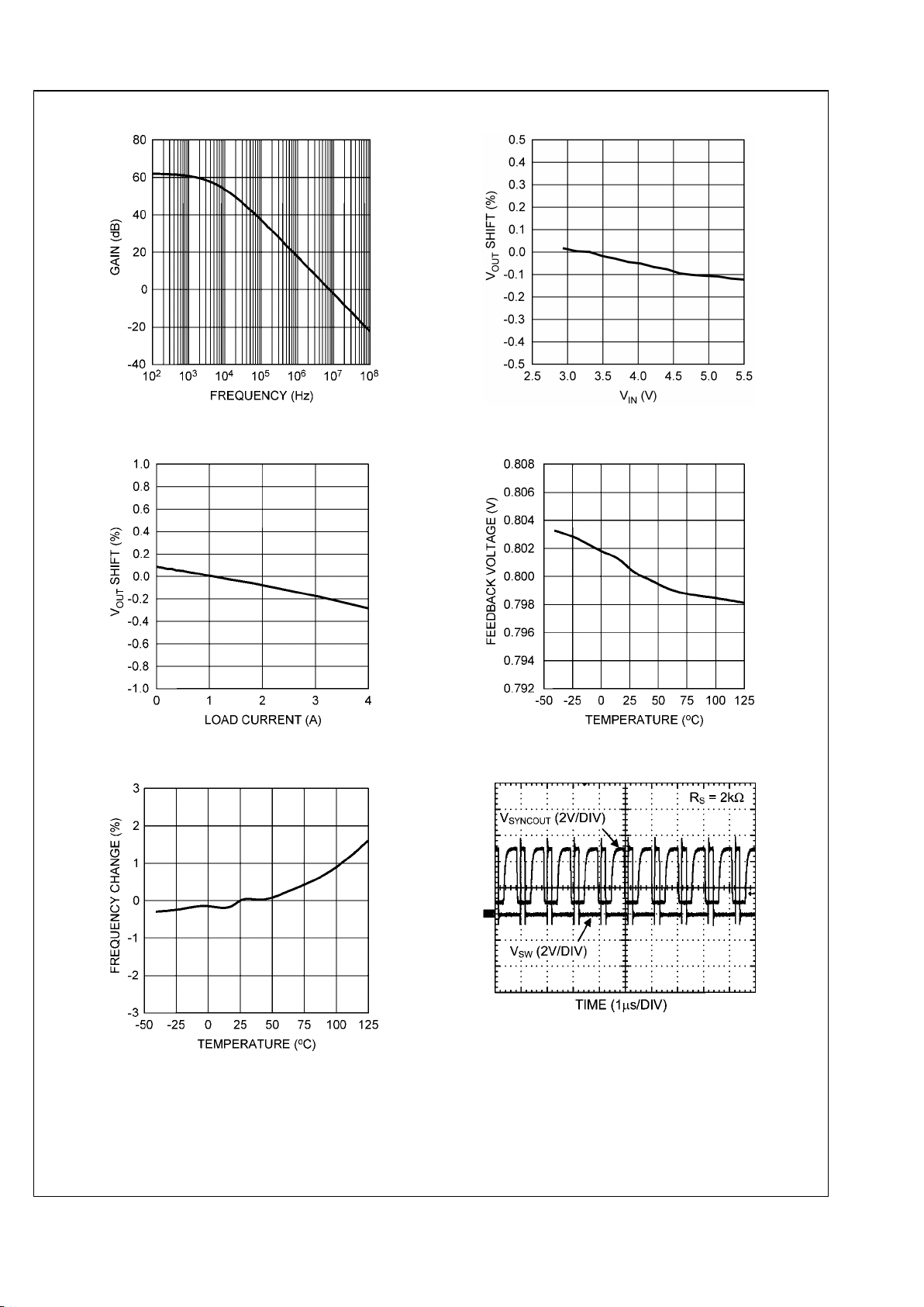
Error Amplifier Gain vs. Frequency
30030836
Line Regulation
30030837
Load Regulation
30030838
Feedback Pin Voltage vs. Temperature
30030851
Switching Frequency vs. Temperature
30030839
Synchronization Output
30030861
5 www.national.com
LM20154

Quiescent Current vs. VIN (Not Switching)
30030840
Shutdown Current vs. Temperature
30030841
Enable Threshold vs. Temperature
30030828
UVLO Threshold vs. Temperature
30030845
Peak Current Limit vs. Temperature
30030842
Peak Current Limit vs. V
OUT
30030854
www.national.com 6
LM20154
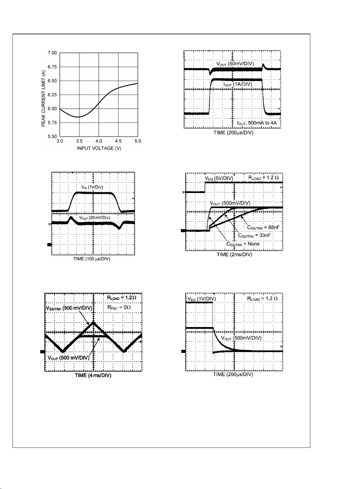
Peak Current Limit vs. V
IN
30030855
Load Transient Response
30030834
Line Transient Response
30030843
Start-Up (Soft-Start)
30030844
Start-Up (Tracking)
30030833
Power Down
30030832
7 www.national.com
LM20154
 Loading...