NSC JM38510R75702SC Datasheet

54AC14
Hex Inverter with Schmitt Trigger Input
General Description
The ’AC14 contains six inverter gates each with a Schmitt
trigger input. The ’AC14 contains six logic inverters which accept standard CMOS input signals and provide standard
CMOS output levels. They are capable of transforming
slowly changing input signals into sharply defined, jitter-free
output signals. In addition, they have a greater noise margin
than conventional inverters.
The ’AC14 has hysteresis between the positive-going and
negative-going input thresholds (typically 1.0V) which is de-
termined internally by transistor ratios and is essentially insensitive to temperature and supply voltage variations.
Features
n ICCreduced by 50
%
n Outputs source/sink 24 mA
n Standard Military Drawing (SMD)
— ’AC14: 5962-87624
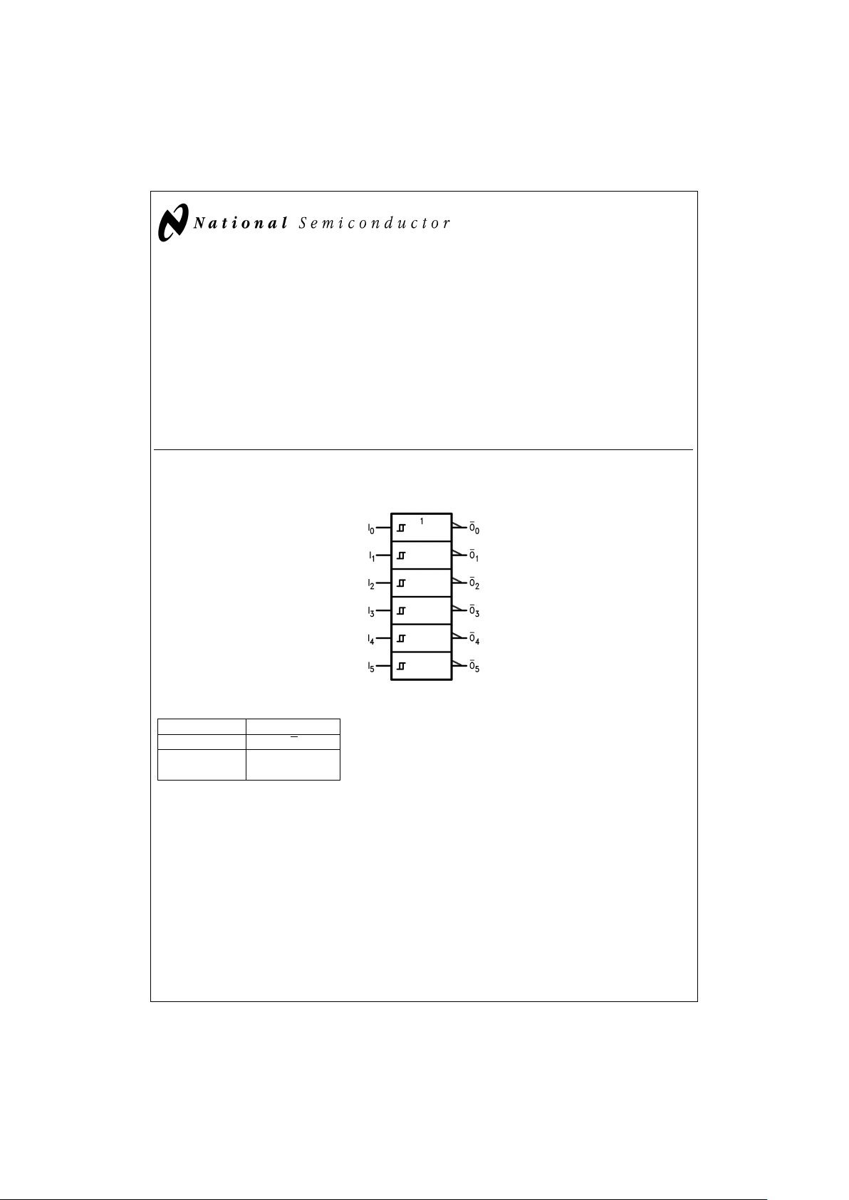
Logic Symbol
Function Table
Input Output
AO
LH
HL
FACT™is a trademark of Fairchild SemiconductorCorporation.
IEEE/IEC
DS100263-1
July 1998
54AC14 Hex Inverter with Schmitt Trigger Input
© 1998 National Semiconductor Corporation DS100263 www.national.com

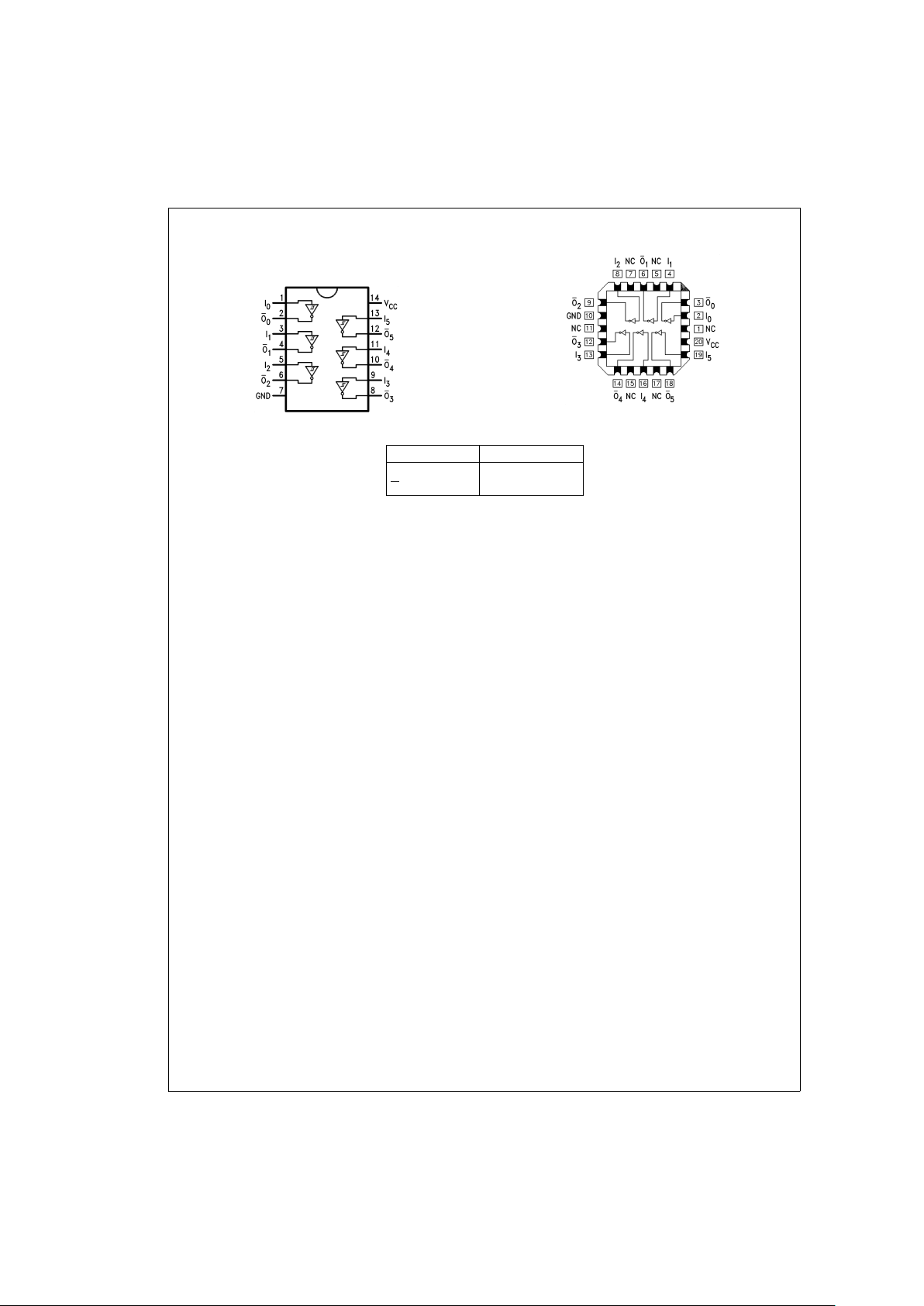
Connection Diagrams
Pin Names Description
I
n
Inputs
O
n
Outputs
Pin Assignment for
DIP and Flatpack
DS100263-2
Pin Assignment for LCC
DS100263-3
www.national.com 2

Absolute Maximum Ratings (Note 1)
If Military/Aerospace specified devices are required,
please contact the National Semiconductor Sales Office/
Distributors for availability and specifications.
Supply Voltage (V
CC
) −0.5V to +7.0V
DC Input Diode Current (I
IK
)
V
I
=
−0.5V −20 mA
V
I
=
V
CC
+ 0.5V +20 mA
DC Input Voltage (V
I
) −0.5V to VCC+ 0.5V
DC Output Diode Current (I
OK
)
V
O
=
−0.5V −20 mA
V
O
=
V
CC
+ 0.5V +20 mA
DC Output Voltage (V
O
) −0.5V to VCC+ 0.5V
DC Output Source
or Sink Current (I
O
)
±
50 mA
DC V
CC
or Ground Current
per Output Pin (I
CC
or I
GND
)
±
50 mA
Storage Temperature (T
STG
) −65˚C to +150˚C
Junction Temperature (T
J
)
CDIP 175˚C
Recommended Operating
Conditions
Supply Voltage (VCC)
’AC 2.0V to 6.0V
Input Voltage (V
I
) 0VtoV
CC
Output Voltage (VO) 0VtoV
CC
Operating Temperature (TA)
54AC −55˚C to +125˚C
Note 1: Absolute maximum ratings are those values beyond which damage
to the device may occur. The databook specifications should be met, without
exception, to ensure that the system design is reliable over its power supply,
temperature, and output/input loading variables. National does not recommend operation of FACT
™
circuits outside databook specifications.
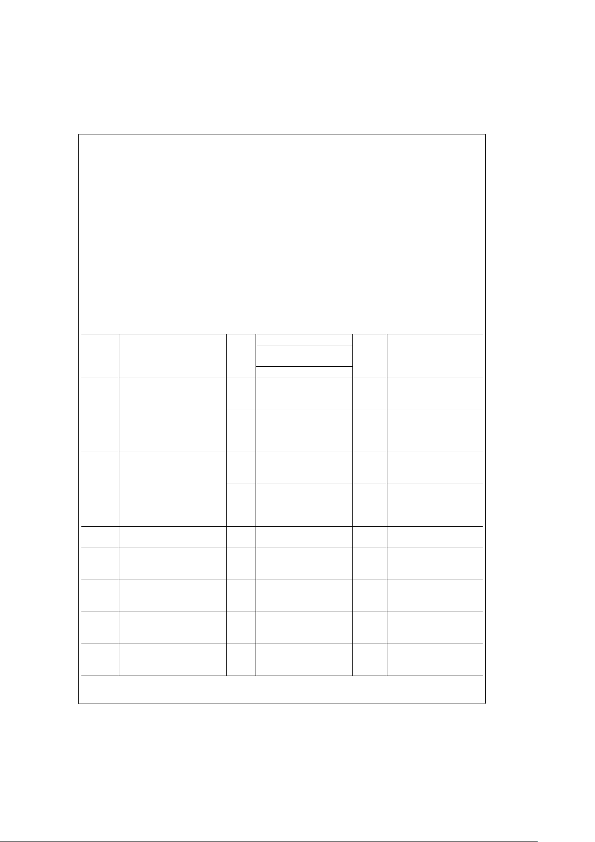
DC Characteristics for ’AC Family Devices
54AC
Symbol Parameter V
CC
T
A
=
−55˚C to +125˚C Units Conditions
(V)
Guaranteed Limits
V
OH
Minimum High Level Output
Voltage
3.0 2.9 I
OUT
=
−50 µA
4.5 4.4 V
5.5 5.4
(Note 2) V
IN
=
V
IL
or V
IH
3.0 2.4 −12 mA
4.5 3.7 V I
OH
−24 mA
5.5 4.7 −24 mA
V
OL
Maximum Low Level Output
Voltage
3.0 0.1 I
OUT
=
50 µA
4.5 0.1 V
5.5 0.1
(Note 2) V
IN
=
V
IL
or V
IH
3.0 0.5 12 mA
4.5 0.5 V I
OL
24 mA
5.5 0.5 24 mA
I
IN
Maximum Input 5.5
±
1.0 µA V
I
=
V
CC
, GND
Leakage Current
V
t+
Maximum Positive 3.0 2.2 T
A
=
Worst Case
Threshold 4.5 3.2 V
5.5 3.9
V
t−
Minimum Negative 3.0 0.5 T
A
=
Worst Case
Threshold 4.5 0.9 V
5.5 1.1
V
h(max)
Maximum Hysteresis 3.0 1.2 T
A
=
Worst Case
4.5 1.4 V
5.5 1.6
V
h(min)
Minimum Hysteresis 3.0 0.3 T
A
=
Worst Case
4.5 0.4 V
5.5 0.5
3 www.national.com
 Loading...