TL/F/6379
54LS85/DM54LS85/DM74LS85 4-Bit Magnitude Comparators
June 1989
54LS85/DM54LS85/DM74LS85
4-Bit Magnitude Comparators
General Description
These 4-bit magnitude comparators perform comparison of
straight binary or BCD codes. Three fully-decoded decisions
about two, 4-bit words (A, B) are made and are externally
available at three outputs. These devices are fully expandable to any number of bits without external gates. Words of
greater length may be compared by connecting comparators in cascade. The A
l
B, AkB, and AeB outputs of a
stage handling less-significant bits are connected to the corresponding inputs of the next stage handling more-significant bits. The stage handling the least-significant bits must
have a high-level voltage applied to the A
e
B input. The
cascading path is implemented with only a two-gate-level
delay to reduce overall comparison times for long words.
Features
Y
Typical power dissipation 52 mW
Y
Typical delay (4-bit words) 24 ns
Y
Alternate Military/Aerospace device (54LS85) is available. Contact a National Semiconductor Sales Office/
Distributor for specifications.
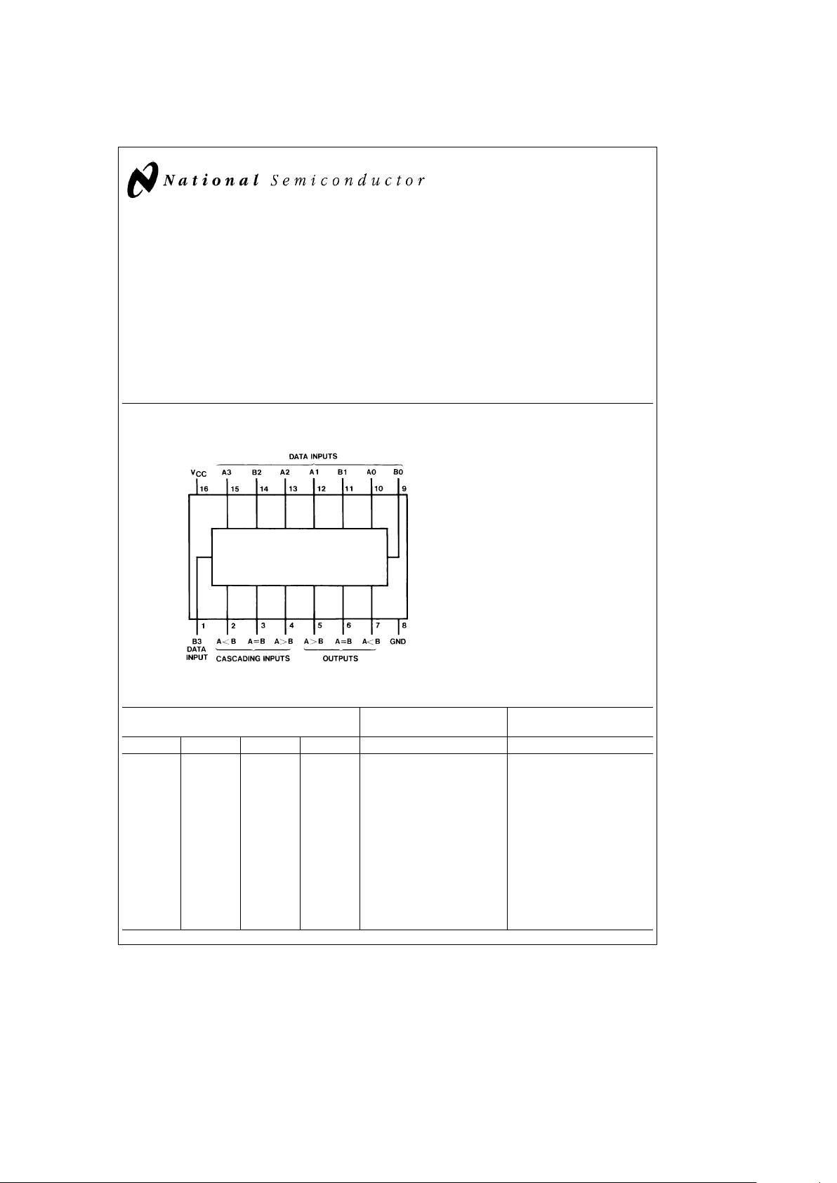
Connection Diagram
Dual-In-Line Package
TL/F/6379– 1
Order Number 54LS85DMQB,
54LS85FMQB, 54LS85LMQB,
DM54LS85J, DM54LS85W,
DM74LS85M or DM74LS85N
See NS Package Number E20A,
J16A, M16A, N16E or W16A
Function Table
Comparing Cascading
Outputs
Inputs Inputs
A3, B3 A2, B2 A1, B1 A0, B0 AlBAkBA
e
BAlBAkBA
e
B
A3lB3 X X X X X X H L L
A3
k
B3 X X X X X X L H L
A3
e
B3 A2lB2 X X X X X H L L
A3
e
B3 A2kB2 X X X X X L H L
A3eB3 A2eB2 A1lB1 X X X X H L L
A3
e
B3 A2eB2 A1kB1 X X X X L H L
A3eB3 A2eB2 A1eB1 A0lB0 X X X H L L
A3
e
B3 A2eB2 A1eB1 A0kB0 X X X L H L
A3
e
B3 A2eB2 A1eB1 A0eB0 H L L H L L
A3
e
B3 A2eB2 A1eB1 A0eB0 L H L L H L
A3
e
B3 A2eB2 A1eB1 A0eB0LLHLLH
A3
e
B3 A2eB2 A1eB1 A0eB0XXHLLH
A3eB3 A2eB2 A1eB1 A0eB0HHLLLL
A3
e
B3 A2eB2 A1eB1 A0eB0LLLHHL
H
e
High Level, LeLow Level, XeDon’t Care
C
1995 National Semiconductor Corporation RRD-B30M105/Printed in U. S. A.

Absolute Maximum Ratings (Note)
If Military/Aerospace specified devices are required,
please contact the National Semiconductor Sales
Office/Distributors for availability and specifications.
Supply Voltage 7V
Input Voltage 7V
Operating Free Air Temperature Range
DM54LS and 54LS
b
55§Ctoa125§C
DM74LS 0
§
Ctoa70§C
Storage Temperature Range
b
65§Ctoa150§C
Note:
The ‘‘Absolute Maximum Ratings’’ are those values
beyond which the safety of the device cannot be guaranteed. The device should not be operated at these limits. The
parametric values defined in the ‘‘Electrical Characteristics’’
table are not guaranteed at the absolute maximum ratings.
The ‘‘Recommended Operating Conditions’’ table will define
the conditions for actual device operation.
Recommended Operating Conditions
Symbol Parameter
DM54LS85 DM74LS85
Units
Min Nom Max Min Nom Max
V
CC
Supply Voltage 4.5 5 5.5 4.75 5 5.25 V
V
IH
High Level Input Voltage 2 2 V
V
IL
Low Level Input Voltage 0.7 0.8 V
I
OH
High Level Output Current
b
0.4
b
0.4 mA
I
OL
Low Level Output Current 4 8 mA
T
A
Free Air Operating Temperature
b
55 125 0 70
§
C
Electrical Characteristics over recommended operating free air temperature range (unless otherwise noted)
Symbol Parameter Conditions Min
Typ
Max Units
(Note 1)
V
I
Input Clamp Voltage V
CC
e
Min, I
I
eb
18 mA
b
1.5 V
V
OH
High Level Output V
CC
e
Min, I
OH
e
Max DM54 2.5 3.4
V
Voltage V
IL
e
Max, V
IH
e
Min
DM74 2.7 3.4
V
OL
Low Level Output V
CC
e
Min, I
OL
e
Max DM54 0.25 0.4
Voltage V
IL
e
Max, V
IH
e
Min
DM74 0.35 0.5 V
I
OL
e
4 mA, V
CC
e
Min DM74 0.25 0.4
I
I
Input Current@Max V
CC
e
Max AkB 0.1
Input Voltage V
I
e
7V
AlB 0.1 mA
Others 0.3
I
IH
High Level Input V
CC
e
Max AkB20
Current V
I
e
2.7V
AlB20mA
Others 60
I
IL
Low Level Input V
CC
e
Max AkB
b
0.4
Current V
I
e
0.4V
AlB
b
0.4 mA
Others
b
1.2
I
OS
Short Circuit V
CC
e
Max DM54
b
20
b
100
mA
Output Current (Note 2)
DM74
b
20
b
100
I
CC
Supply Current V
CC
e
Max (Note 3) 10 20 mA
Note 1: All typicals are at V
CC
e
5V, T
A
e
25§C.
Note 2: Not more than one output should be shorted at a time, and the duration should not exceed one second.
Note 3: I
CC
is measured with all outputs open, AeB grounded and all other inputs at 4.5V.
2

Switching Characteristics at V
CC
e
5V and T
A
e
25§C (See Section 1 for Test Waveforms and Output Load)
From To Number of
R
L
e
2kX
Symbol Parameter Input Output Gate Levels C
L
e
15 pF C
L
e
50 pF Units
Min Max Min Max
t
PLH
Propagation Delay Time Any A or B AkB,
33642
Low-to-High Level Output Data Input A
l
Bns
A
e
B 4 40 40
t
PHL
Propagation Delay Time Any A or B AkB,
33040
High-to-Low Level Output Data Input AlBns
A
e
B 4 30 40
t
PLH
Propagation Delay Time AkB
A
l
B 1 22 26 ns
Low-to-High Level Output or A
e
B
t
PHL
Propagation Delay Time AkB
A
l
B 1 17 26 ns
High-to-Low Level Output or AeB
t
PLH
Propagation Delay Time
A
e
BA
e
B 2 20 25 ns
Low-to-High Level Output
t
PHL
Propagation Delay Time
A
e
BA
e
B 2 17 26 ns
High-to-Low Level Output
t
PLH
Propagation Delay Time AlB
A
k
B 1 22 26 ns
Low-to-High Level Output or AeB
t
PHL
Propagation Delay Time AlB
A
k
B 1 17 26 ns
High-to-Low Level Output or AeB
3
 Loading...