

NSC DS90CR218MTDX, DS90CR218MTD Datasheet
DS90CR217/DS90CR218
+3.3V Rising Edge Data Strobe LVDS 21-Bit Channel
Link - 75 MHz
General Description
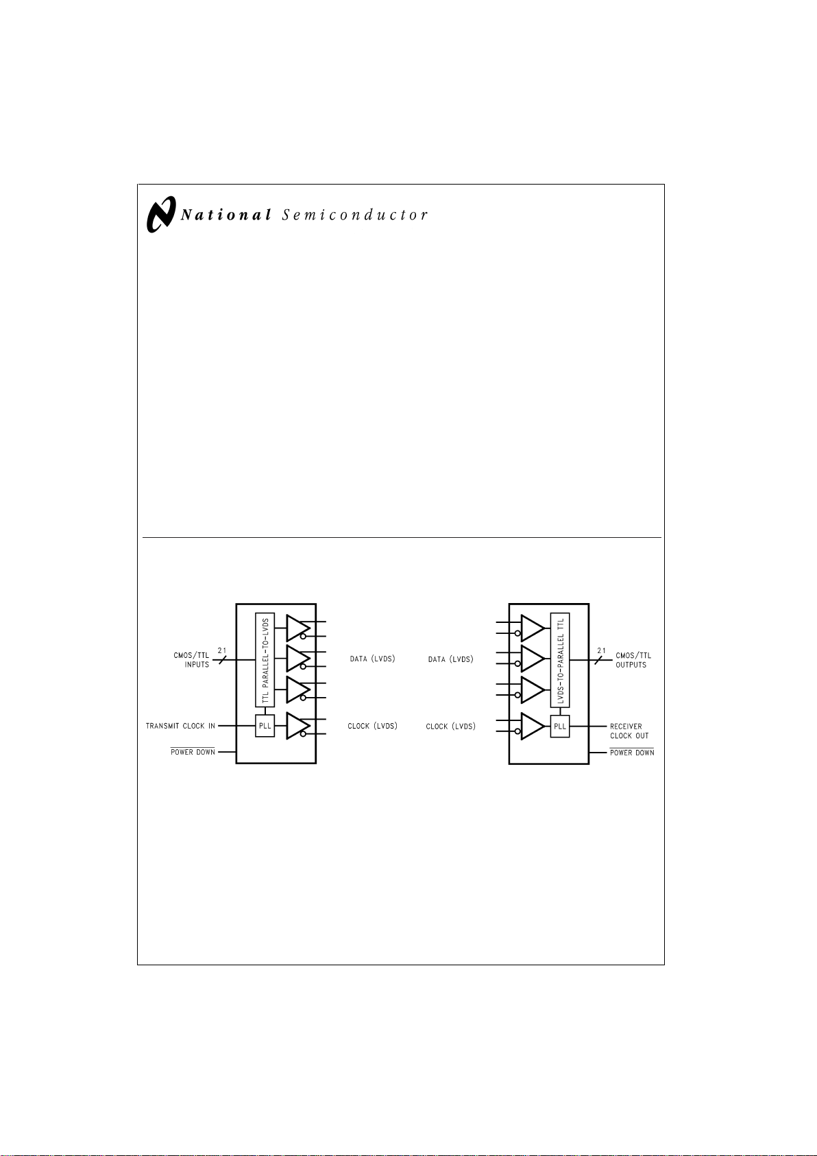
The DS90CR217 transmitter converts 21 bits of CMOS/TTL
data into three LVDS (Low Voltage Differential Signaling)
data streams.Aphase-locked transmit clockis transmitted in
parallel with thedata streams over a fourth LVDS link.Every
cycle of the transmit clock 21 bits of input data are sampled
and transmitted. The DS90CR218 receiver converts the
three LVDS data streams back into 21 bits of CMOS/TTL
data.At a transmit clockfrequency of 75 MHz, 21 bits ofTTL
data are transmitted at a rate of 525 Mbps per LVDS data
channel. Usinga 75 MHz clock,the data throughputis 1.575
Gbit/s (197 Mbytes/sec).
This chipset is an ideal means to solve EMI and cable size
problems associated with wide, high speed TTL interfaces.
Features
n 20 to 75 MHz shift clock support
n 50%duty cycle on receiver output clock
n Best–in–Class Set & Hold Times on TxINPUTs and
RxOUTPUTs
n Low power consumption
n Tx + Rx Power-down mode
<
400µW (max)
n
±
1V common mode range (around +1.2V)
n Narrow bus reduces cable size and cost
n Up to 1.575 Gbps throughput
n Up to 197 Megabytes/sec bandwidth
n 345 mV (typ) swing LVDS devices for low EMI
n PLL requires no external components
n Rising edge data strobe
n Compatible with TIA/EIA-644 LVDS standard
n Low profile 48-lead TSSOP package
Block Diagrams
TRI-STATE®is a registered trademark of National Semiconductor Corporation.
DS90CR217
DS100871-1
Order Number DS90CR217MTD
See NS Package Number MTD48
DS90CR218
DS100871-27
Order Number DS90CR218MTD
See NS Package Number MTD48
November 1999
DS90CR217/DS90CR218 +3.3V Rising Edge Data Strobe LVDS 21-Bit Channel Link-75 MHz
© 1999 National Semiconductor Corporation DS100871 www.national.com
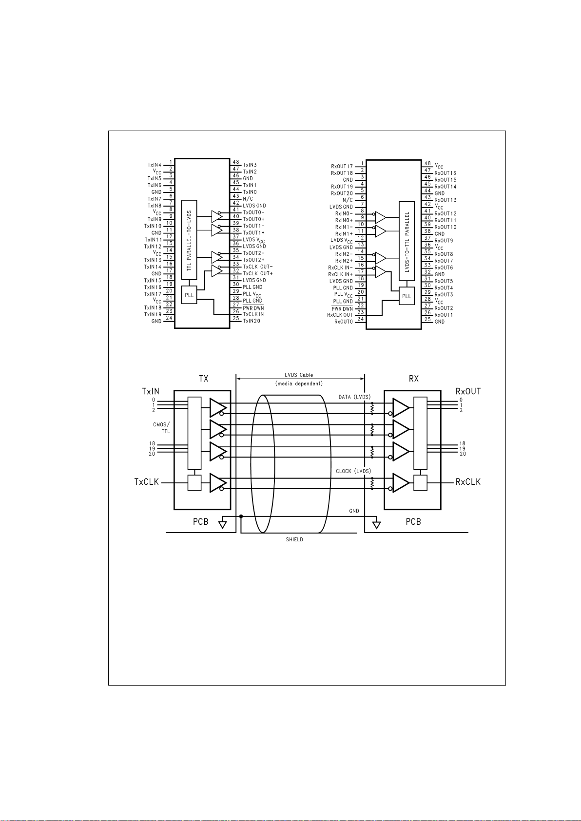
Pin Diagrams
Typical Application
DS100871-21
DS90CR217
DS100871-22
DS90CR218
DS100871-23
DS90CR217/DS90CR218
www.national.com 2
Absolute Maximum Ratings (Note 1)
If Military/Aerospace specified devices are required,
please contactthe National Semiconductor Sales Office/
Distributors for availability and specifications.
Supply Voltage (V
CC
) −0.3V to +4V
CMOS/TTL Input Voltage −0.5V to (V
CC
+ 0.3V)
CMOS/TTL Output Voltage −0.3V to (V
CC
+ 0.3V)
LVDS Receiver Input Voltage −0.3V to (V
CC
+ 0.3V)
LVDS Driver Output Voltage −0.3V to (V
CC
+ 0.3V)
LVDS Output Short
Circuit Duration Continuous
Junction Temperature +150˚C
Storage Temperature Range −65˚C to +150˚C
Lead Temperature
(Soldering, 4 sec.) +260˚C
Maximum Package Power Dissipation
@
+25˚C
MTD48 (TSSOP) Package:
DS90CR217 1.98 W
DS90CR218 1.89 W
Package Derating
DS90CR217 16 mW/˚C above +25˚C
DS90CR218 15 mW/˚C above +25˚C
ESD Rating
(HBM, 1.5kΩ, 100pF)
>
7kV
(EIAJ, 0Ω, 200pF)
>
700V
Latch Up Tolerance
@
25˚C
>
±
300mA
Recommended Operating
Conditions
Min Nom Max Units
Supply Voltage (V
CC
) 3.0 3.3 3.6 V
Operating Free Air
Temperature (T
A
) −10 +25 +70 ˚C
Receiver Input Range 0 2.4 V
Supply Noise Voltage (V
CC
) 100 mV
PP
Electrical Characteristics
Over recommended operating supply and temperature ranges unless otherwise specified
Symbol Parameter Conditions Min Typ Max Units
CMOS/TTL DC SPECIFICATIONS
V
IH
High Level Input Voltage 2.0 V
CC
V
V
IL
Low Level Input Voltage GND 0.8 V
V
OH
High Level Output Voltage IOH= −0.4 mA 2.7 3.3 V
V
OL
Low Level Output Voltage IOL= 2 mA 0.06 0.3 V
V
CL
Input Clamp Voltage ICL= −18 mA −0.79 −1.5 V
I
IN
Input Current VIN= 0.4V, 2.5V or V
CC
+1.8 +10 µA
V
IN
= GND −10 0 µA
I
OS
Output Short Circuit Current V
OUT
= 0V −60 −120 mA
LVDS DRIVER DC SPECIFICATIONS
V
OD
Differential Output Voltage RL= 100Ω 250 290 450 mV
∆V
OD
Change in VODbetween
Complimentary Output States
35 mV
V
OS
Offset Voltage (Note 4) 1.125 1.25 1.375 V
∆V
OS
Change in VOSbetween
Complimentary Output States
35 mV
I
OS
Output Short Circuit Current V
OUT
= 0V, −3.5 −5 mA
R
L
= 100Ω
I
OZ
Output TRI-STATE®Current PWR DWN = 0V,
±
1
±
10 µA
V
OUT
=0VorV
CC
LVDS RECEIVER DC SPECIFICATIONS
V
TH
Differential Input High Threshold VCM= +1.2V +100 mV
V
TL
Differential Input Low Threshold −100 mV
I
IN
Input Current VIN= +2.4V, VCC= 3.6V
±
10 µA
V
IN
= 0V, VCC= 3.6V
±
10 µA
TRANSMITTER SUPPLY CURRENT
I
CCTW
Transmitter Supply Current
Worst Case (with Loads)
RL= 100Ω,
C
L
= 5 pF,
Worst Case
Pattern
(
Figures 1, 2
)
f = 33 MHz 28 42 mA
f = 40 MHz 29 47 mA
f = 66 MHz 34 52 mA
f = 75 MHz 39 57 mA
DS90CR217/DS90CR218
www.national.com3
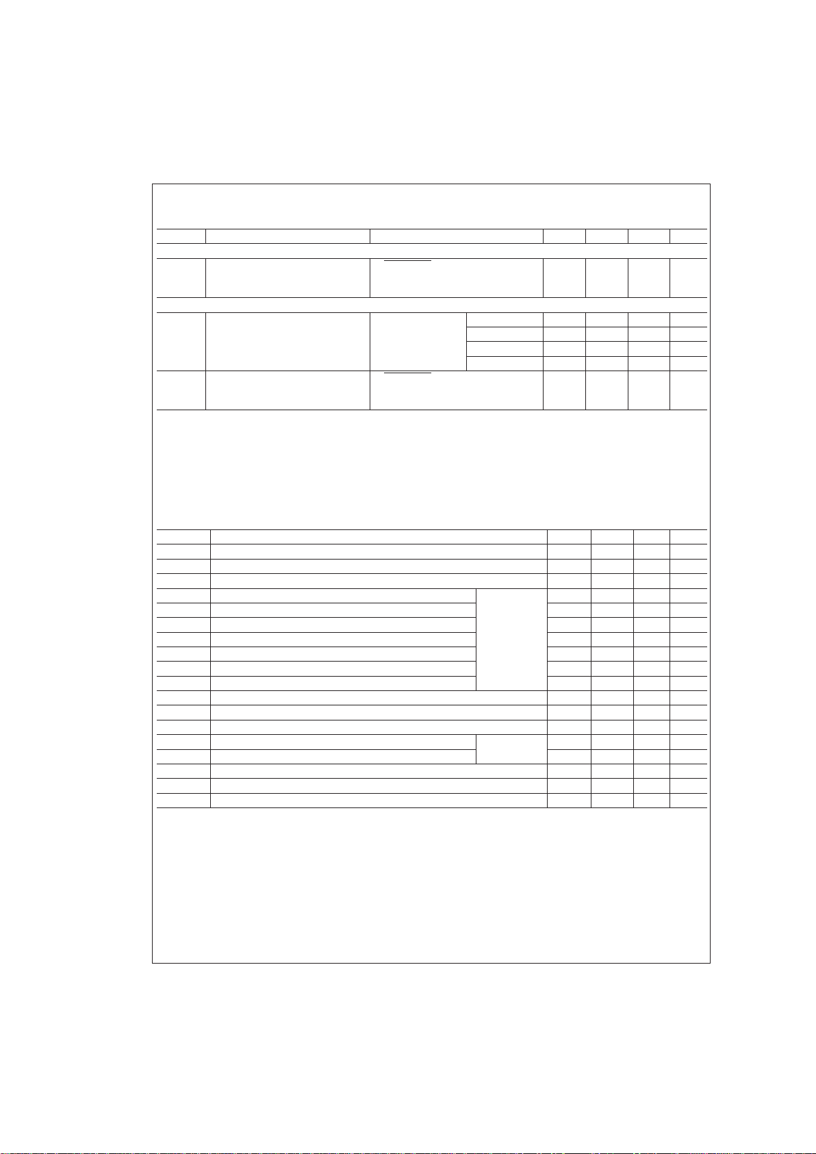
Electrical Characteristics (Continued)
Over recommended operating supply and temperature ranges unless otherwise specified
Symbol Parameter Conditions Min Typ Max Units
TRANSMITTER SUPPLY CURRENT
I
CCTZ
Transmitter Supply Current
Power Down
PWR DWN = Low
Driver Outputs in TRI-STATE
under Powerdown Mode
10 55 µA
RECEIVER SUPPLY CURRENT
I
CCRW
Receiver Supply Current Worst
Case
CL= 8 pF,
Worst Case
Pattern
(
Figures 1, 3
)
f = 33 MHz 49 60 mA
f = 40 MHz 53 65 mA
f = 66 MHz 78 95 mA
f = 75 MHz 90 105 mA
I
CCRZ
Receiver Supply Current Power
Down
PWR DWN = Low
Receiver Outputs Stay Low during
Powerdown Mode
15 55 µA
Note 1: “Absolute Maximum Ratings” are those values beyond which the safety of the device cannot be guaranteed. They are not meant to imply that the device
should be operated at these limits. The tables of “Electrical Characteristics” specify conditions for device operation.
Note 2: Typical values are given for V
CC
= 3.3V and TA= +25˚C.
Note 3: Current into device pins is defined as positive. Current out of device pins is defined as negative. Voltages arereferenced toground unlessotherwise specified (except V
OD
and ∆VOD).
Note 4: V
OS
previously referred as VCM.
Transmitter Switching Characteristics
Over recommended operating supply and temperature ranges unless otherwise specified
Symbol Parameter Min Typ Max Units
LLHT LVDS Low-to-High Transition Time (
Figure 2
) 0.75 1.5 ns
LHLT LVDS High-to-Low Transition Time (
Figure 2
) 0.75 1.5 ns
TCIT TxCLK IN Transition Time (
Figure 4
) 1.0 6.0 ns
TPPos0 Transmitter Output Pulse Position for Bit0 (
Figure 15
) f = 75 MHz −0.20 0 0.20 ns
TPPos1 Transmitter Output Pulse Position for Bit1 1.71 1.91 2.11 ns
TPPos2 Transmitter Output Pulse Position for Bit2 3.61 3.81 4.01 ns
TPPos3 Transmitter Output Pulse Position for Bit3 5.51 5.71 5.91 ns
TPPos4 Transmitter Output Pulse Position for Bit4 7.42 7.62 7.82 ns
TPPos5 Transmitter Output Pulse Position for Bit5 9.32 9.52 9.72 ns
TPPos6 Transmitter Output Pulse Position for Bit6 11.23 11.43 11.63 ns
TCIP TxCLK IN Period (
Figure 6
) 13.33 T 50 ns
TCIH TxCLK IN High Time (
Figure 6
) 0.35T 0.5T 0.65T ns
TCIL TxCLK IN Low Time (
Figure 6
) 0.35T 0.5T 0.65T ns
TSTC TxIN Setup to TxCLK IN (
Figure 6
) f = 75 MHz 2.5 ns
THTC TxIN Hold to TxCLK IN (
Figure 6
)0ns
TCCD TxCLK IN to TxCLK OUT Delay
@
25˚C,VCC=3.3V (
Figure 8
) 3.8 6.3 ns
TPLLS Transmitter Phase Lock Loop Set (
Figure 10
)10ms
TPDD Transmitter Powerdown Delay (
Figure 13
) 100 ns
DS90CR217/DS90CR218
www.national.com 4
Receiver Switching Characteristics
Over recommended operating supply and temperature ranges unless otherwise specified
Symbol Parameter Min Typ Max Units
CLHT CMOS/TTL Low-to-High Transition Time (
Figure 3
) 2.0 3.5 ns
CHLT CMOS/TTL High-to-Low Transition Time (
Figure 3
) 1.8 3.5 ns
RSPos0 Receiver Input Strobe Position for Bit 0 (
Figure 16
) f = 75 MHz 0.58 0.95 1.32 ns
RSPos1 Receiver Input Strobe Position for Bit 1 2.49 2.86 3.23 ns
RSPos2 Receiver Input Strobe Position for Bit 2 4.39 4.76 5.13 ns
RSPos3 Receiver Input Strobe Position for Bit 3 6.30 6.67 7.04 ns
RSPos4 Receiver Input Strobe Position for Bit 4 8.20 8.57 8.94 ns
RSPos5 Receiver Input Strobe Position for Bit 5 10.11 10.48 10.85 ns
RSPos6 Receiver Input Strobe Position for Bit 6 12.01 12.38 12.75 ns
RSKM RxIN Skew Margin (Note 5) (
Figure 17
) f = 75 MHz 380 ps
RCOP RxCLK OUT Period (
Figure 7
) 13.33 T 50 ns
RCOH RxCLK OUT High Time (
Figure 7
) f = 75 MHz 3.6 5 6.0 ns
RCOL RxCLK OUT Low Time (
Figure 7
) 3.6 5 6.0 ns
RSRC RxOUT Setup to RxCLK OUT (
Figure 7
) 3.5 ns
RHRC RxOUT Hold to RxCLK OUT (
Figure 7
) 3.5 ns
RCCD RxCLK IN to RxCLK OUT Delay
@
25˚C, VCC= 3.3V (Note 6)(
Figure 9
) 3.4 5.0 7.3 ns
RPLLS Receiver Phase Lock Loop Set (
Figure 11
)10ms
RPDD Receiver Powerdown Delay (
Figure 14
)1µs
Note 5: Receiver Skew Marginis definedas the validdata sampling region at thereceiver inputs. Thismargin takes into account thetransmitter pulse positions(min
and max) and the receiver input setup and hold time (internal data sampling window). This margin allows LVDS interconnect skew, inter-symbol interference (both
dependent on type/length of cable), and source clock jitter less than 250 ps.
Note 6: Totallatency for thechannel link chipset is afunction of clock period andgate delays throughthe transmitter(TCCD) and receiver(RCCD). The total latency
for the 217/287 transmitter and 218/288 receiver is: (T + TCCD) + (2
*
T + RCCD), where T=Clock period.
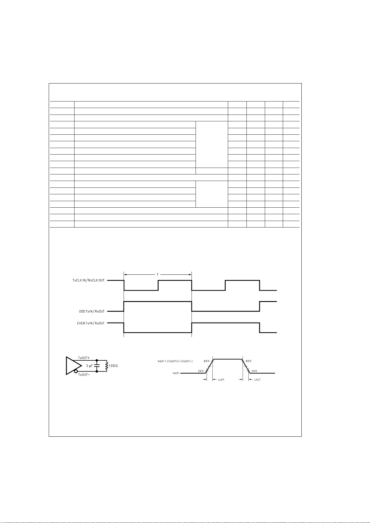
AC Timing Diagrams
DS100871-2
FIGURE 1. “Worst Case” Test Pattern
DS100871-3
DS100871-4
FIGURE 2. DS90CR217 (Transmitter) LVDS Output Load and Transition Times
DS90CR217/DS90CR218
www.national.com5
 Loading...