

DS90C383/DS90CF384
+3.3V Programmable LVDS Transmitter 24-Bit Flat Panel
Display (FPD) Link—65 MHz, +3.3V LVDS Receiver
24-Bit Flat Panel Display (FPD) Link—65 MHz
General Description
The DS90C383 transmitter converts 28 bits of CMOS/TTL
data into fourLVDS(Low Voltage Differential Signaling) data
streams. A phase-locked transmit clock is transmitted in parallel with the data streams over a fifth LVDSlink. Every cycle
of the transmit clock 28 bits of input data are sampled and
transmitted. The DS90CF384 receiver converts the LVDS
data streams back into 28 bits of CMOS/TTL data. At a transmit clock frequency of 65 MHz, 24 bits of RGB data and 3
bits of LCD timing and control data (FPLINE, FPFRAME,
DRDY) are transmitted at a rate of 455 Mbps per LVDS data
channel. Using a 65 MHz clock, the data throughputs is 227
Mbytes/sec. The transmitter is offered with programmable
edge data strobes for convenient interface with a variety of
graphics controllers. The transmitter can be programmed for
Rising edge strobe or Falling edge strobe through a dedicated pin. A Rising edge transmitter will inter-operate with a
Falling edge receiver (DS90CF384) without any translation
logic. The DS90CF384 is also offered in 64 ball, 0.8mm fine
pitch ball grid array(FBGA) package which provides a 44
%
reduction in PCB footprint (available Q3, 1999).
This chipset is an ideal means to solve EMI and cable size
problems associated with wide, high speed TTL interfaces.
Features
n 20 to 65 MHz shift clock support
n Programmable transmitter (DS90C383) strobe select
(Rising or Falling edge strobe)
n Single 3.3V supply
n Chipset (Tx + Rx) power consumption
<
250 mW (typ)
n Power-down mode (
<
0.5 mW total)
n Single pixel per clock XGA (1024x768) ready
n Supports VGA, SVGA, XGA and higher addressability.
n Up to 227 Megabytes/sec bandwidth
n Up to 1.8 Gbps throughput
n Narrow bus reduces cable size and cost
n 290 mV swing LVDS devices for low EMI
n PLL requires no external components
n Low profile 56-lead TSSOP package.
n DS90CF384 also available in 64 ball, 0.8mm fine pitch
ball grid array(FBGA) package
n Falling edge data strobe Receiver
n Compatible with TIA/EIA-644 LVDS standard
n ESD rating
>
7kV
n Operating Temperature: −40˚C to +85˚C
Block Diagrams
TRI-STATE®is a registered trademark of National Semiconductor Corporation.
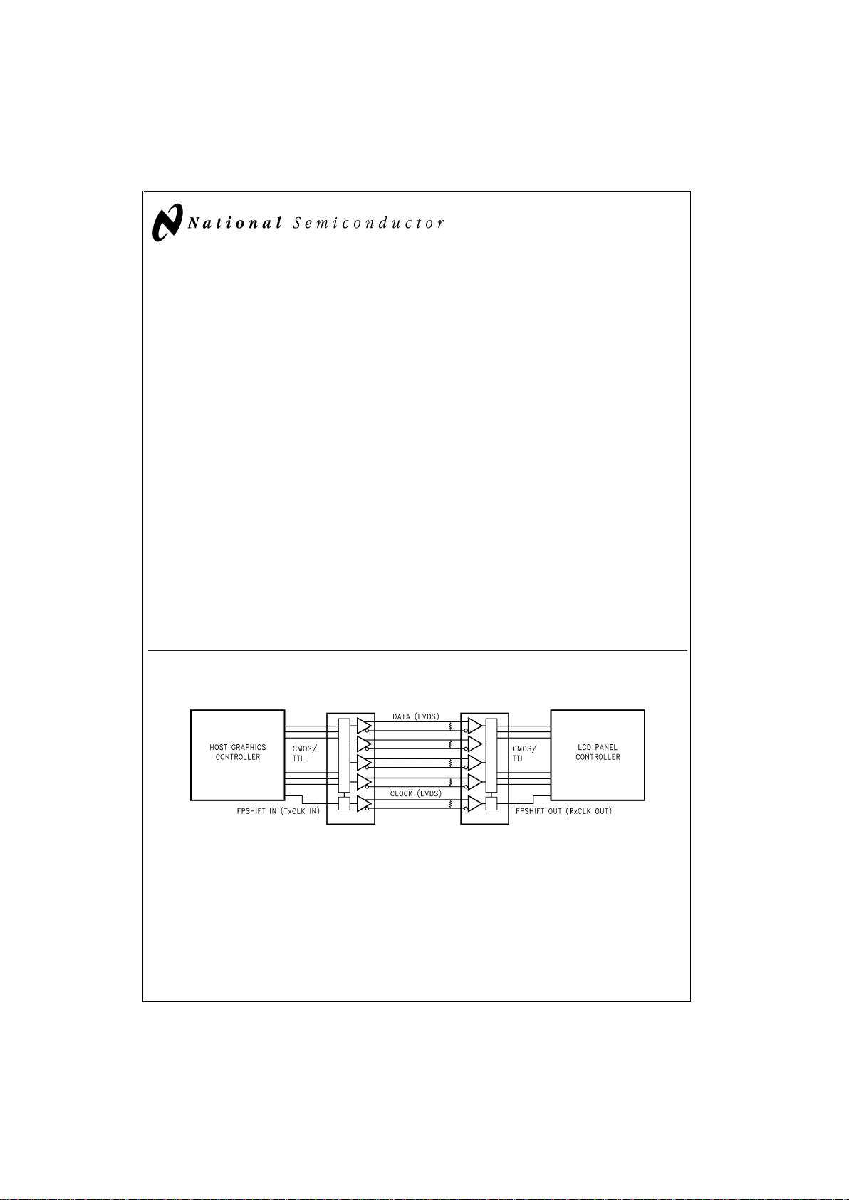
Application
DS012887-2
September 1999
DS90C383/DS90CF384 +3.3V Programmable LVDS 24-Bit-Color Flat Panel Display (FPD)
Link— 65 MHz
© 1999 National Semiconductor Corporation DS012887 www.national.com
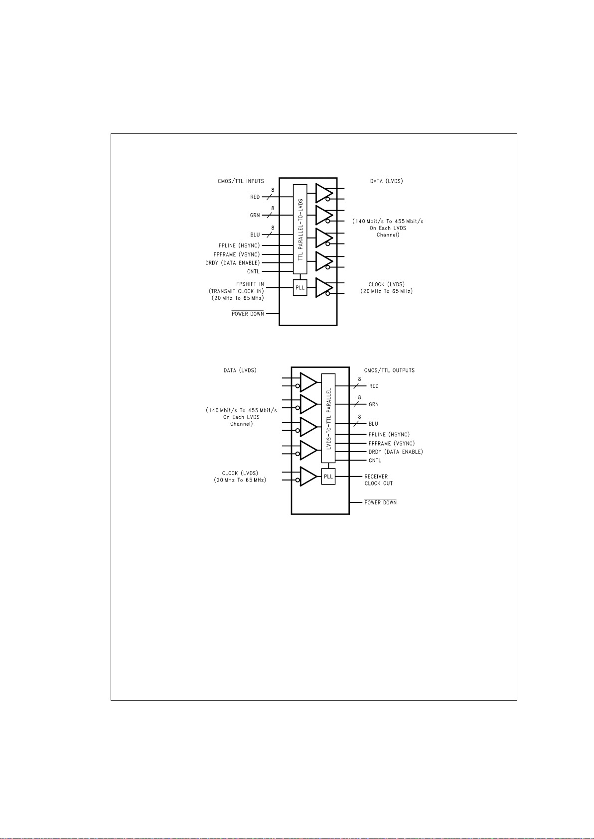
Block Diagrams (Continued)
DS90C383
DS012887-1
Order Number DS90C383MTD
See NS Package Number MTD56
DS90CF384
DS012887-24
Order Number DS90CF384MTD or DS90CF384SLC
See NS Package Number MTD56 or SLC64A
www.national.com 2
Absolute Maximum Ratings (Note 1)
If Military/Aerospace specified devices are required,
please contact the National Semiconductor Sales Office/
Distributors for availability and specifications.
Supply Voltage (V
CC
) −0.3V to +4V
CMOS/TTL Input Voltage −0.3V to (V
CC
+ 0.3V)
CMOS/TTL Output Voltage −0.3V to (V
CC
+ 0.3V)
LVDS Receiver Input Voltage −0.3V to (V
CC
+ 0.3V)
LVDS Driver Output Voltage −0.3V to (V
CC
+ 0.3V)
LVDS Output Short Circuit
Duration Continuous
Junction Temperature +150˚C
Storage Temperature −65˚C to +150˚C
Lead Temperature
(Soldering, 4 sec for TSSOP) +260˚C
Solder Reflow Temperature
(20 sec for FBGA) +220˚C
Maximum Package Power Dissipation Capacity 25˚C
MTD56 (TSSOP) Package:
DS90C383MTD 1.63 W
DS90CF384MTD 1.61 W
Package Derating:
DS90C383MTD 12.5 mW/˚C above +25˚C
DS90CF384MTD 12.4 mW/˚C above +25˚C
Maximum Package Power Dissipation Capacity 25˚C
SLC64A Package:
DS90CF384SLC 2.0 W
Package Derating:
DS90CF384SLC 10.2 mW/˚C above +25˚C
ESD Rating
(HBM, 1.5 kΩ, 100 pF)
>
7kV
Recommended Operating
Conditions
Min Nom Max Units
Supply Voltage (V
CC
) 3.0 3.3 3.6 V
Operating Free Air
Temperature (T
A
) −40 +25 +85 ˚C
Receiver Input Range 0 2.4 V
Supply Noise Voltage (V
CC
) 100 mV
PP
Electrical Characteristics
Over recommended operating supply and temperature ranges unless otherwise specified.
Symbol Parameter Conditions Min Typ Max Units
CMOS/TTL DC SPECIFICATIONS
V
IH
High Level Input Voltage 2.0 V
CC
V
V
IL
Low Level Input Voltage GND 0.8 V
V
OH
High Level Output Voltage IOH= −0.4 mA 2.7 3.3 V
V
OL
Low Level Output Voltage IOL= 2 mA 0.06 0.3 V
V
CL
Input Clamp Voltage ICL= −18 mA −0.79 −1.5 V
I
IN
Input Current VIN=VCC, GND, 2.5V or 0.4V
±
5.1
±
10 µA
I
OS
Output Short Circuit Current V
OUT
= 0V −60 −120 mA
LVDS DC SPECIFICATIONS
V
OD
Differential Output Voltage RL= 100Ω 250 345 450 mV
∆V
OD
Change in VODbetween 35 mV
complimentary output states
V
OS
Offset Voltage (Note 4) 1.125 1.25 1.375 V
∆V
OS
Change in VOSbetween 35 mV
complimentary output states
I
OS
Output Short Circuit Current V
OUT
= 0V, RL= 100Ω −3.5 −5 mA
I
OZ
Output TRI-STATE®Current Power Down = 0V,
±
1
±
10 µA
V
OUT
=0VorV
CC
V
TH
Differential Input High Threshold VCM= +1.2V +100 mV
V
TL
Differential Input Low Threshold −100 mV
I
IN
Input Current VIN= +2.4V, VCC= 3.6V
±
10 µA
V
IN
= 0V, VCC= 3.6V
±
10 µA
TRANSMITTER SUPPLY CURRENT
ICCTW Transmitter Supply Current R
L
= 100Ω,
C
L
= 5 pF,
f = 32.5 MHz 31 45 mA
Worst Case Worst Case Pattern f = 37.5 MHz 32 50 mA
(Figures 1, 3 )
,TA=
−40˚C to +85˚C
f = 65 MHz 42 55 mA
www.national.com3
Electrical Characteristics (Continued)
Over recommended operating supply and temperature ranges unless otherwise specified.
Symbol Parameter Conditions Min Typ Max Units
TRANSMITTER SUPPLY CURRENT
ICCTG Transmitter Supply Current R
L
= 100Ω,
C
L
= 5 pF,
f = 32.5 MHz 23 35 mA
16 Grayscale 16 Grayscale Pattern f = 37.5 MHz 28 40 mA
(Figures 2, 3 )
,TA=
−40˚C to +85˚C
f = 65 MHz 31 45 mA
ICCTZ Transmitter Supply Current Power Down = Low
10 55 µA
Power Down Driver Outputs in TRI-STATE
®
under
Power Down Mode
RECEIVER SUPPLY CURRENT
ICCRW Receiver Supply Current C
L
= 8 pF, f = 32.5 MHz 49 65 mA
Worst Case Worst Case Pattern f = 37.5 MHz 53 70 mA
(Figures 1, 4 )
,TA=
−40˚C to +85˚C
f = 65 MHz 78 105 mA
ICCRG Receiver Supply Current, C
L
= 8 pF, f = 32.5 MHz 28 45 mA
16 Grayscale 16 Grayscale Pattern f = 37.5 MHz 30 47 mA
(Figures 2, 4 )
,TA=
−40˚C to +85˚C
f = 65 MHz 43 60 mA
ICCRZ Receiver Supply Current Power Down = Low
10 55 µA
Power Down Receiver Outputs Stay Low during
Power Down Mode
Note 1: “Absolute Maximum Ratings” are those values beyond which the safety of the device cannot be guaranteed. They are not meant to imply that the device
should be operated at these limits. The tables of “Electrical Characteristics” specify conditions for device operation.
Note 2: Typical values are given for V
CC
= 3.3V and TA= +25C.
Note 3: Current into device pins is defined as positive. Current out of device pins is defined as negative. Voltages are referenced to ground unless otherwise specified (except V
OD
and ∆VOD).
Note 4: V
OS
previously referred as VCM.
Transmitter Switching Characteristics
Over recommended operating supply and −40˚C to +85˚C ranges unless otherwise specified
Symbol Parameter Min Typ Max Units
LLHT LVDS Low-to-High Transition Time
(Figure 3 )
0.75 1.5 ns
LHLT LVDS High-to-Low Transition Time
(Figure 3 )
0.75 1.5 ns
TCIT TxCLK IN Transition Time
(Figure 5 )
5ns
TCCS TxOUT Channel-to-Channel Skew
(Figure 6 )
250 ps
TPPos0 Transmitter Output Pulse Position for Bit 0
(Figure 17 )
f = 65 MHz −0.4 0 0.3 ns
TPPos1 Transmitter Output Pulse Position for Bit 1 1.8 2.2 2.5 ns
TPPos2 Transmitter Output Pulse Position for Bit 2 4.0 4.4 4.7 ns
TPPos3 Transmitter Output Pulse Position for Bit 3 6.2 6.6 6.9 ns
TPPos4 Transmitter Output Pulse Position for Bit 4 8.4 8.8 9.1 ns
TPPos5 Transmitter Output Pulse Position for Bit 5 10.6 11 11.3 ns
TPPos6 Transmitter Output Pulse Position for Bit 6 12.8 13.2 13.5 ns
TCIP TxCLK IN Period
(Figure 7)
15 T 50 ns
TCIH TxCLK IN High Time
(Figure 7)
0.35T 0.5T 0.65T ns
TCIL TxCLK IN Low Time
(Figure 7)
0.35T 0.5T 0.65T ns
TSTC TxIN Setup to TxCLK IN
(Figure 7 )
f = 65 MHz 2.5 ns
THTC TxIN Hold to TxCLK IN
(Figure 7 )
0ns
TCCD TxCLK IN to TxCLK OUT Delay 25˚C, V
CC
= 3.3V
(Figure 9 )
3.0 3.7 5.5 ns
TPLLS Transmitter Phase Lock Loop Set
(Figure 11 )
10 ms
TPDD Transmitter Power Down Delay
(Figure 15 )
100 ns
www.national.com 4
Receiver Switching Characteristics
Over recommended operating supply and −40˚C to +85˚C ranges unless otherwise specified
Symbol Parameter Min Typ Max Units
CLHT CMOS/TTL Low-to-High Transition Time
(Figure 4 )
2.2 5.0 ns
CHLT CMOS/TTL High-to-Low Transition Time
(Figure 4 )
2.2 5.0 ns
RSPos0 Receiver Input Strobe Position for Bit 0
(Figure 18 )
f = 65 MHz 0.7 1.1 1.4 ns
RSPos1 Receiver Input Strobe Position for Bit 1 2.9 3.3 3.6 ns
RSPos2 Receiver Input Strobe Position for Bit 2 5.1 5.5 5.8 ns
RSPos3 Receiver Input Strobe Position for Bit 3 7.3 7.7 8.0 ns
RSPos4 Receiver Input Strobe Position for Bit 4 9.5 9.9 10.2 ns
RSPos5 Receiver Input Strobe Position for Bit 5 11.7 12.1 12.4 ns
RSPos6 Receiver Input Strobe Position for Bit 6 13.9 14.3 14.6 ns
RSKM RxIN Skew Margin (Note 5)
(Figure 19 )
f = 65 MHz 400 ps
RCOP RxCLK OUT Period
(Figure 8)
15 T 50 ns
RCOH RxCLK OUT High Time
(Figure 8 )
f = 65 MHz 7.3 8.6 ns
RCOL RxCLK OUT Low Time
(Figure 8)
3.45 4.9 ns
RSRC RxOUT Setup to RxCLK OUT
(Figure 8 )
2.5 6.9 ns
RHRC RxOUT Hold to RxCLK OUT
(Figure 8 )
2.5 5.7 ns
RCCD RxCLK IN to RxCLK OUT Delay 25˚C, V
CC
= 3.3V
(Figure 10 )
5.0 7.1 9.0 ns
RPLLS Receiver Phase Lock Loop Set
(Figure 12 )
10 ms
RPDD Receiver Power Down Delay
(Figure 16 )
1µs
Note 5: Receiver Skew Margin is defined as the valid data sampling region at the receiver inputs. This margin takes into account the transmitter pulse positions (min
and max) and the receiver input setup and hold time (internal data sampling window-RSPOS). This margin allows for LVDSinterconnect skew, inter-symbol interference (both dependent on type/length of cable), and clock jitter (less than 250 ps).
AC Timing Diagrams
DS012887-3
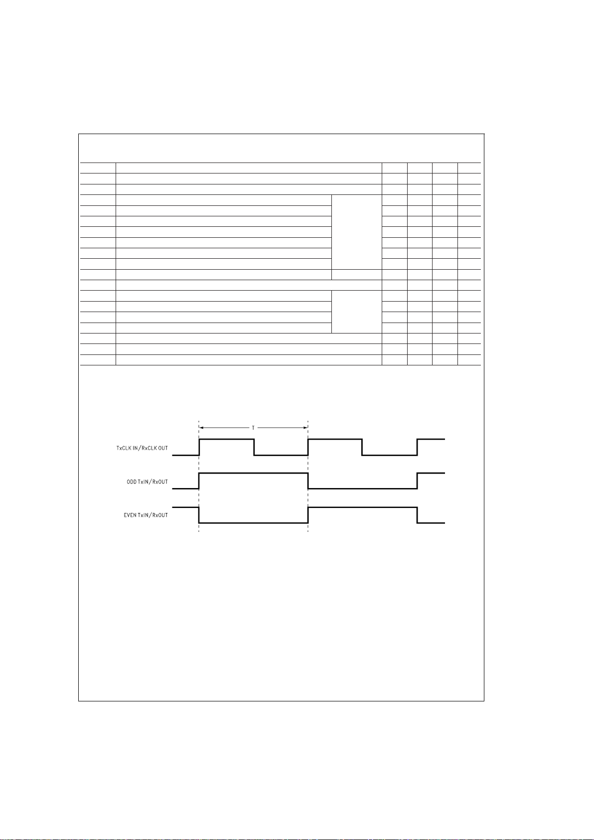
FIGURE 1. “Worst Case” Test Pattern
www.national.com5
AC Timing Diagrams (Continued)
Note 6: The worst case test pattern produces a maximum toggling of digital circuits, LVDS I/O and CMOS/TTL I/O.
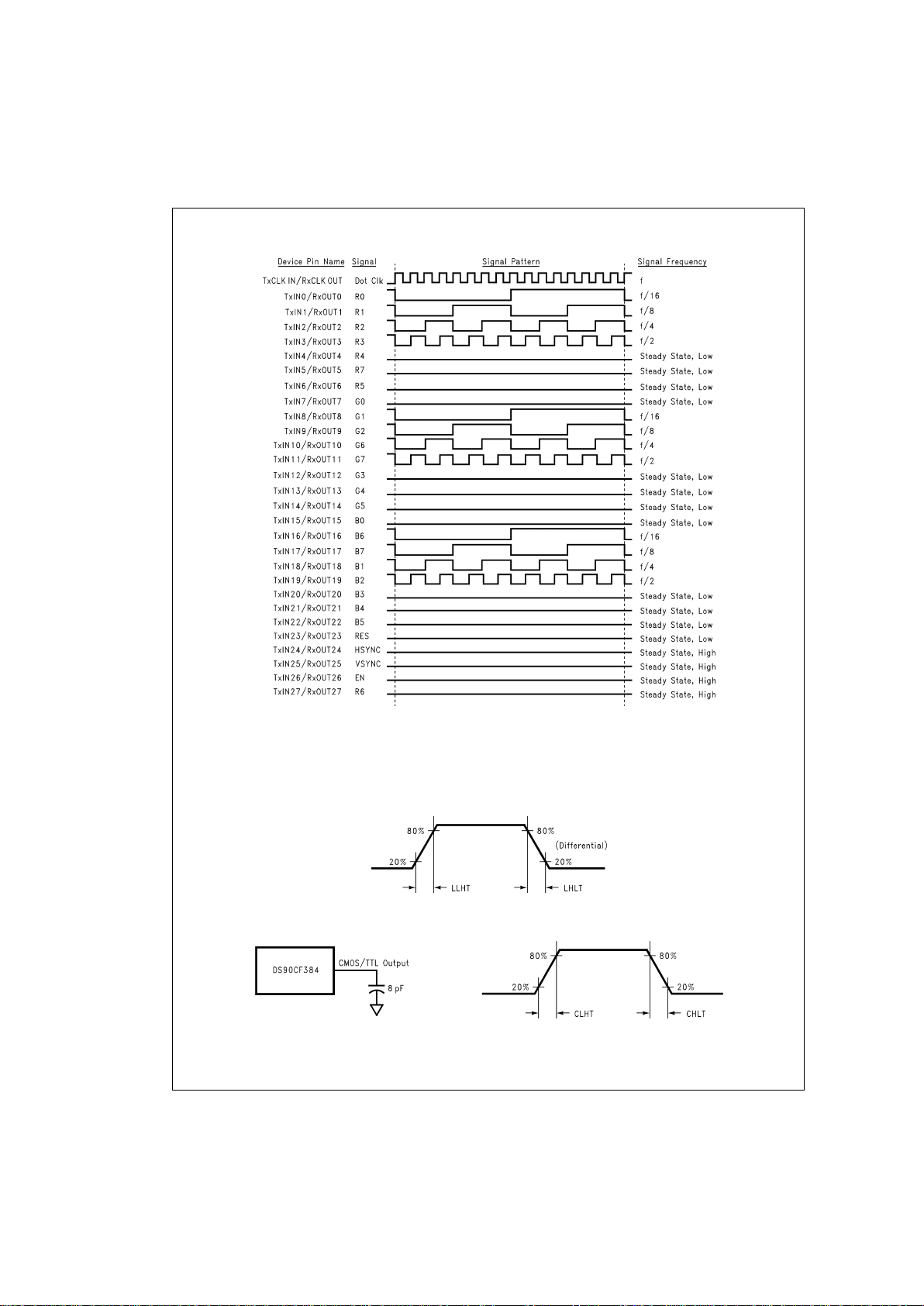
Note 7: The 16 grayscale test pattern tests device power consumption for a “typical” LCD display pattern. The test pattern approximates signal switching needed
to produce groups of 16 vertical stripes across the display.
Note 8:
Figures 1, 2
show a falling edge data strobe (TxCLK IN/RxCLK OUT).
Note 9: Recommended pin to signal mapping. Customer may choose to define differently.
DS012887-4
FIGURE 2. “16 Grayscale” Test Pattern (Notes 6, 7, 8, 9)
DS012887-5
FIGURE 3. DS90C383 (Transmitter) LVDS Output Load and Transition Times
DS012887-6
FIGURE 4. DS90CF384 (Receiver) CMOS/TTL Output Load and Transition Times
www.national.com 6
 Loading...