

NSC DS75492MX, DS75492M, DS75492N Datasheet
TL/F/5830
DS75491 MOS-to-LED Quad Segment Driver DS75492 MOS-to-LED Hex Digit Driver
February 1995
DS75491 MOS-to-LED Quad Segment Driver
DS75492 MOS-to-LED Hex Digit Driver
General Description
The DS75491 and DS75492 are interface circuits designed
to be used in conjunction with MOS integrated circuits and
common-cathode LEDs in serially addressed multi-digit displays. The number of drivers required for this time-multiplexed system is minimized as a result of the segment-address-and-digit-scan method of LED drive.
Features
Y
50 mA source or sink capability per driver (DS75491)
Y
250 mA sink capability per driver (DS75492)
Y
MOS compatability (low input current)
Y
Low standby power
Y
High-gain Darlington circuits
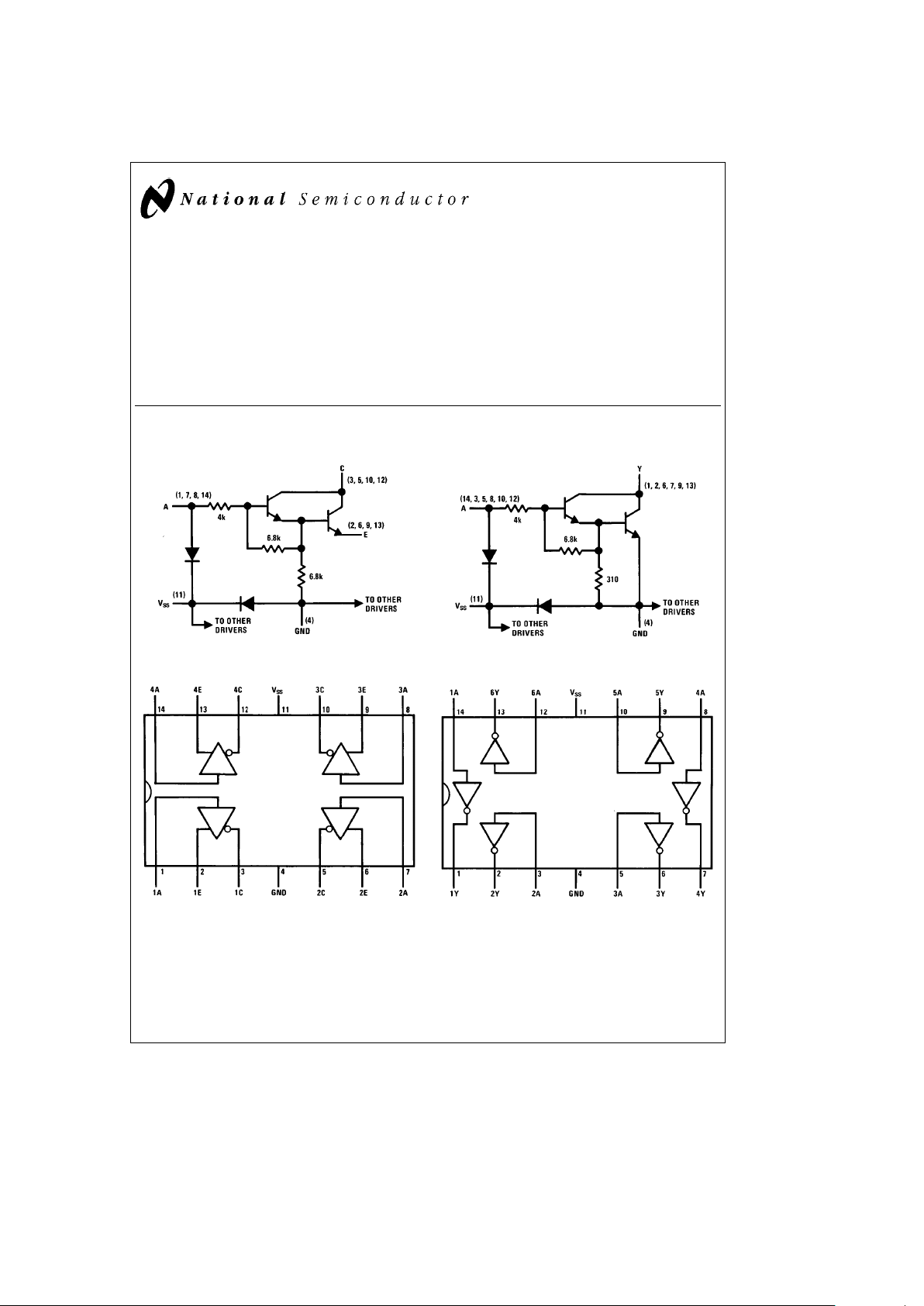
Schematic and Connection Diagrams
DS75491 (each driver)
TL/F/5830– 1
DS75492 (each driver)
TL/F/5830– 2
DS75491 Dual-In-Line Package
TL/F/5830– 3
Top View
DS75492 Dual-In-Line Package
TL/F/5830– 4
Top View
Order Number DS75491N, DS75492M or DS75492N
See NS Package Number M14A or N14A
C
1995 National Semiconductor Corporation RRD-B30M105/Printed in U. S. A.
Absolute Maximum Ratings (Note 1)
If Military/Aerospace specified devices are required,
please contact the National Semiconductor Sales
Office/Distributors for availability and specifications.
DS75491 DS75492
Input Voltage Range (Note 4)
b
5V to V
SS
Collector Output Voltage (Note 5) 10V 10V
Collector Output to Input Voltage 10V 10V
Emitter to Ground Voltage (V
I
t
5V) 10V
Emitter to Input Voltage 5V
Voltage at V
SS
Terminal with Respect
to any Other Device Terminal 10V 10V
Collector Output Current
Each Collector Output 50 mA 250 mA
All Collector Outputs 200 mA 600 mA
DS75491 DS75492
Continuous Total Dissipation 600 mW 600 mW
Operating Temperature Range 0
§
Ctoa70§C
Storage Temperature Range
b
65§Ctoa150§C
Lead Temp. (Soldering, 10 sec) 300§C 300§C
Maximum Power Dissipation
at 25
§
C
Molded Package 1207 mW* 1280 mW
²
*Derate molded package 9.66 mW/§C above 25§C.
²
Derate molded package 10.24 mW/§C above 25§C.
Electrical Characteristics V
SS
e
10V (Notes 2 and 3)
Symbol Parameter Conditions Min Typ Max Units
DS75491
V
CE ON
‘‘ON’’ State Collector Emitter Voltage Inpute8.5V through 1 kX,T
A
e
25§C 0.9 1.2 V
V
E
e
5V, I
C
e
50 mA
T
A
e
0–70§C 1.5 V
I
C OFF
‘‘OFF’’ State Collector Current V
C
e
10V, I
IN
e
40 mA 100 mA
V
E
e
0V
V
IN
e
0.7V 100 mA
I
I
Input Current at Maximum Input Voltage V
IN
e
10V, V
E
e
0V, I
C
e
20 mA 2.2 3.3 mA
I
E
Emitter Reverse Current V
IN
e
0V, V
E
e
5V, I
C
e
0 mA 100 mA
I
SS
Current Into VSSTerminal 1mA
DS75492
V
OL
Low Level Output Voltage Inpute6.5V through 1 kX,T
A
e
25§C 0.9 1.2 V
I
OUT
e
250 mA
T
A
e
0–70§C 1.5 V
I
OH
High Level Output Current V
OH
e
10V I
IN
e
40 mA 200 mA
V
IN
e
0.5V 200 mA
I
I
Input Current at Maximum Input Voltage V
IN
e
10V, I
OL
e
20 mA 2.2 3.3 mA
I
SS
Current Into VSSTerminal 1mA
Switching Characteristics V
SS
e
7.5V, T
A
e
25§C
Symbol Parameter Conditions Min Typ Max Units
DS75491
t
PLH
Propagation Delay Time, Low-to-High Level Output (Collector) V
IH
e
4.5V, V
E
e
0V, 100 ns
t
PHL
Propagation Delay Time, High-to-Low Level Output (Collector)
R
L
e
200X,C
L
e
15 pF
20 ns
DS75492
t
PLH
Propagation Delay Time, Low-to-High Level Output V
IH
e
7.5V, R
L
e
39X, 300 ns
t
PHL
Propagation Delay Time, High-to-Low Level Output
C
L
e
15 pF
30 ns
Note 1: ‘‘Absolute Maximum Ratings’’ are those values beyond which the safety of the device cannot be guaranteed. Except for ‘‘Operating Temperature Range’’
they are not meant to imply that the devices should be operated at these limits. The table of ‘‘Electrical Characteristics’’ provides conditions for actual device
operation.
Note 2: Unless otherwise specified min/max limits apply across the 0
§
Ctoa70§C temperature range for the DS75491 and DS75492.
Note 3: All currents into device pins shown as positive, out of device pins as negative, all voltages referenced to ground unless otherwise noted. All values shown
as max or min on absolute value basis.
Note 4: The input is the only device terminal which may be negative with respect to ground.
Note 5: Voltage values are with respect to network ground terminal unless otherwise noted.
2
 Loading...