

DS75451/2/3
Series Dual Peripheral Drivers
DS75451/2/3 Series Dual Peripheral Drivers
February 2000
General Description
The DS7545X series of dual peripheral drivers is a family of
versatile devices designed for use in systems that use TTL
logic. Typical applications include high speed logic buffers,
power drivers, relay drivers, lamp drivers, MOS drivers, bus
drivers and memory drivers.
The DS75451, DS75452 and DS75453 are dual peripheral
AND, NAND and NOR drivers, respectively, (positive logic)
with the output of the logic gates internally connected to the
bases of the NPN output transistors.
Features
n 300 mA output current capability
n High voltage outputs
n No output latch-up at 20V
n High speed switching
n Choice of logic function
n TTL compatible diode-clamped inputs
n Standard supply voltages
n Replaces TI “A” and “B” series
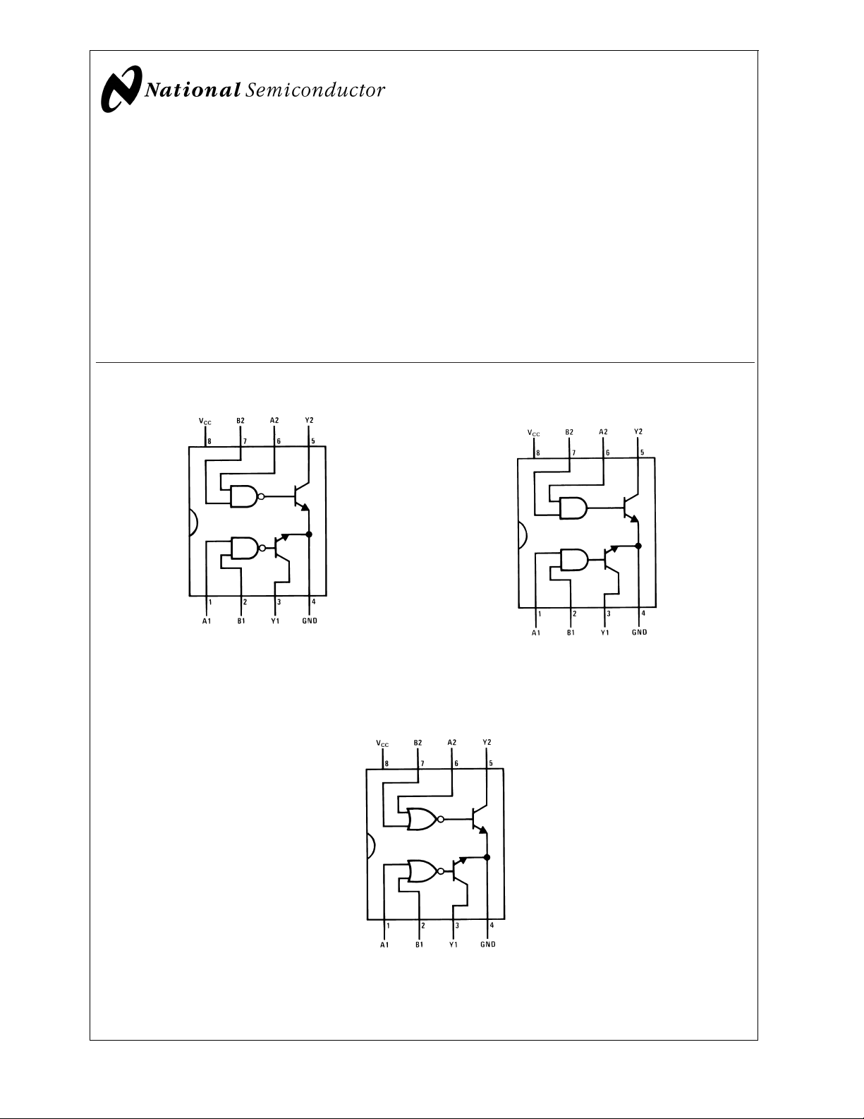
Connection Diagrams (Dual-In-Line and Metal Can Packages)
DS005824-2
*
See (Note 5) and Appendix E regarding S.O. package power dissipation
constraints.
Top View
Order Number DS75451M or DS75451N
See NS Package Numbers M08A
*
See (Note 5) and Appendix E regarding S.O. package power dissipation constraints.
Top View
Order Number DS75453M or DS75453N
See NS Package Numbers M08A
DS005824-3
Top View
Order Number DS75452M or DS75452N
*
or N08E
DS005824-4
*
or N08E
© 2001 National Semiconductor Corporation DS005824 www.national.com
Absolute Maximum Ratings (Note 1)
If Military/Aerospace specified devices are required,
please contact the National Semiconductor Sales Office/
Distributors for availability and specifications.
DS75451/2/3
Supply Voltage, (V
Input Voltage 5.5V
Inter-Emitter Voltage (Note 3) 5.5V
Output Voltage (Note 4) 30V
Output Current (Note 5) 300 mA
Maximum Power (Note 5)
Dissipation
) (Note 2) 7.0V
CC
†
at 25˚C
Molded DIP Package 957 mW
SO Package 632 mW
Storage Temperature Range −65˚C to +150˚C
Lead Temperature (Soldering, 4 sec.) 260˚C
Operating Conditions
Min Max Units
Supply Voltage, (V
Temperature, (T
†
Derate molded package 7.7 mW/˚C above 25˚C, derate SO package 7.56
mW/˚C above 25˚C.
) 4.75 5.25 V
CC
) 0 +70 ˚C
A
Electrical Characteristics
(Notes 6, 7)
Symbol Parameter Conditions Min Typ Max Units
V
IH
V
IL
V
I
V
OL
I
OH
I
I
I
IH
I
IL
I
CCH
I
CCL
High-Level Input Voltage (
Figure 7
)2V
Low-Level Input Voltage 0.8 V
Input Clamp Voltage VCC= Min, II= −12 mA −1.5 V
Low-Level Output Voltage VCC=
Min,
Figure 7
(
High-Level Output Current VCC=
Min,
Figure 7
(
Input Current at Maximum
VCC= Max, VI= 5.5V, (
= 0.8V IOL= 100 mA DS75451, DS75453 0.25 0.4 V
V
IL
I
= 300 mA DS75451, DS75453 0.5 0.7 V
)
V
=2V IOL= 100 mA DS75452 0.25 0.4 V
IH
= 30V VIH= 2V DS75451, DS75453
V
OH
)
OL
I
= 300 mA DS75452 0.5 0.7 V
OL
V
= 0.8V DS75452
IL
Figure 9
)
100 µA
100 µA
Input Voltage
High-Level Input Current VCC= Max, VI= 2.4V, (
Low-Level Input Current VCC= Max, VI= 0.4V, (
Supply Current, Outputs
High
Supply Current, Outputs
Low
VCC=
Max,
Figure
(
)
10
VCC=
Max,
Figure
(
)
10
= 5V DS75451
V
I
V
= 0V DS75452
I
V
= 5V DS75453
I
= 0V DS75451
V
I
V
= 5V DS75452
I
V
= 0V DS75453
I
Figure 9
Figure 8
)40µA
) −1 −1.6 mA
711mA
11 14 mA
811mA
52 65 mA
56 71 mA
54 68 mA
1mA
Switching Characteristics
(VCC=5V,TA= 25˚C)
Symbol Parameter Conditions Min Typ Max Units
t
PLH
t
PHL
t
TLH
t
THL
V
OH
Propagation Delay Time, Low-to-High
Level Output
Propagation Delay Time, High-to-Low
Level Output
Transition Time, Low-to-High Level
Output
Transition Time, High-to-Low Level
Output
High-Level Output Voltage after
CL= 15 pF, RL=50Ω,
≈200 mA, (
I
O
CL= 15 pF, RL=50Ω,
≈200 mA, (
I
O
CL= 15 pF, RL=50Ω,IO≈200 mA,
Figure 14
(
)
CL= 15 pF, RL=50Ω,IO≈200 mA,
(Figure 14 )
VS= 20V, IO≈ 300 mA, (
Switching
www.national.com 2
Figure 14
Figure 14
DS75451 18 25 ns
)
DS75452 26 35 ns
DS75453 18 25 ns
DS75451 18 25 ns
)
DS75452 24 35 ns
DS75453 16 25 ns
58 ns
712 ns
Figure 15
)
V
− 6.5 mV
S
Switching Characteristics (Continued)
Note 1: “Absolute Maximum Ratings” are those values beyond which the safety of the device cannot be guaranteed. Except for “Operating Temperature Range”
they are not meant to imply that the devices should be operated at these limits. The table of “Electrical Characteristics” provides conditions for actual device
operation.
Note 2: Voltage values are with respect to network ground terminal unless otherwise specified.
Note 3: The voltage between two emitters of a multiple-emitter transistor.
Note 4: The maximum voltage which should be applied to any output when it is in the “OFF” state.
Note 5: Both halves of these dual circuitsmayconduct rated current simultaneously; however, power dissipation averaged over a short time interval must fall within
the continuous dissipation rating.
Note 6: Unless otherwise specified min/max limits apply across 0˚C to +70˚C range. All typicals are given for V
Note 7: All currents into device pins shown as positive, out of device pins as negative, all voltages referenced to ground unless otherwise noted. All values shown
as max or min on absolute value basis.
= +5V and TA= 25˚C.
CC
Truth Tables (H = high level, L = low level)
DS75451
AB Y
L L L (ON State)
L H L (ON State)
H L L (ON State)
H H H (OFF State)
DS75452
AB Y
L L H (OFF State)
L H H (OFF State)
H L H (OFF State)
H H L (ON State)
DS75451/2/3
DS75453
AB Y
L L L (ON State)
L H H (OFF State)
H L H (OFF State)
H H H (OFF State)
www.national.com3
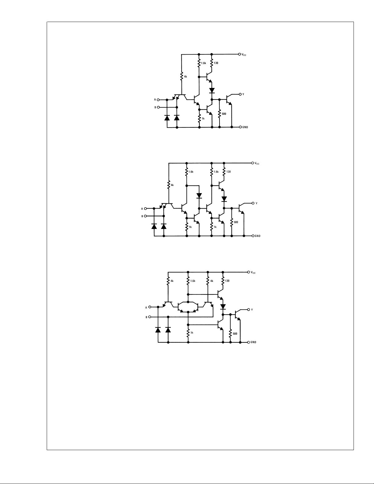
Schematic Diagrams
DS75451/2/3
Resistor values shown are nominal.
DS75451
DS005824-11
DS75452
Resistor values shown are nominal.
Resistor values shown are nominal.
DS005824-12
DS75453
DS005824-13
www.national.com 4
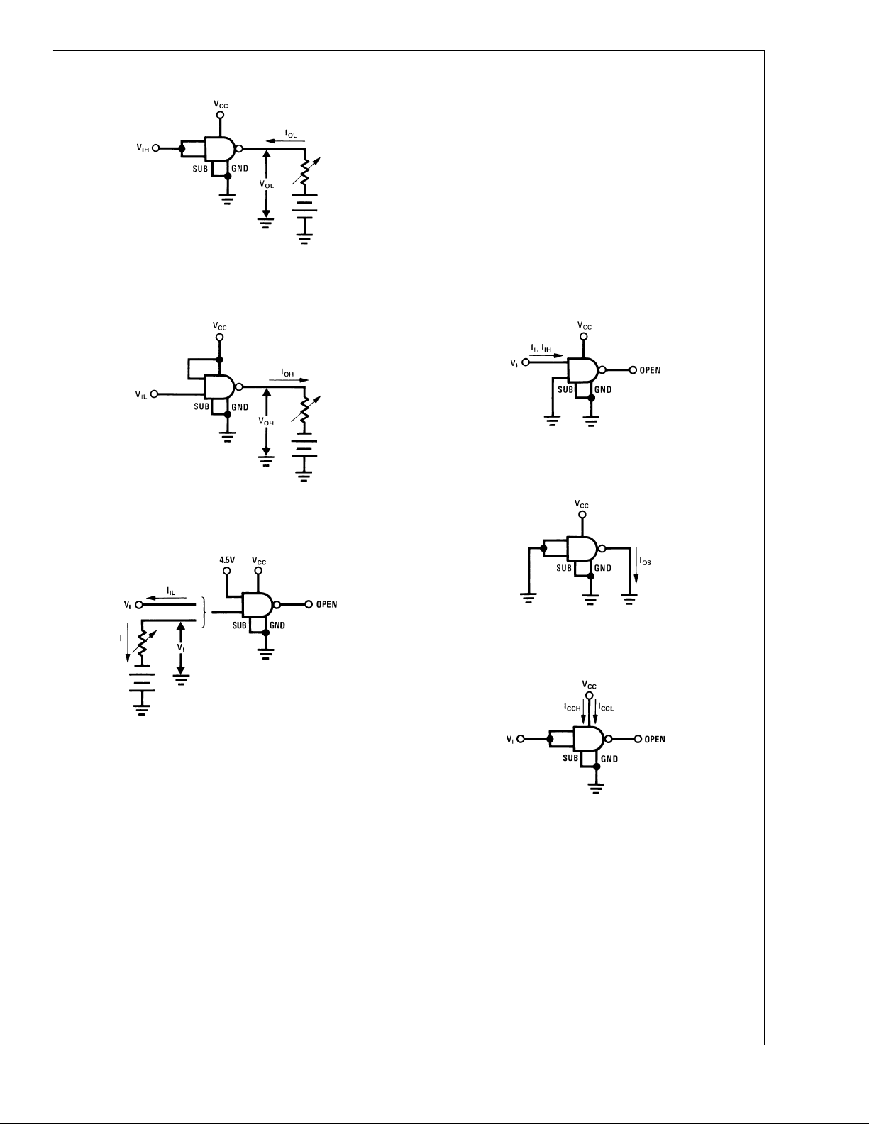
DC Test Circuits
Both inputs is tested simultaneously.
Each input is tested separately.
FIGURE 2. VIL,V
DS005824-15
DS005824-16
OH
FIGURE 1. VIH,V
Each input is tested separately.
DS75451/2/3
OL
DS005824-18
FIGURE 4. II,I
IH
Each input is tested separately.
FIGURE 3. VI,I
IL
DS005824-17
Each input is tested separately.
FIGURE 5. I
Both gates are tested simultaneously.
FIGURE 6. I
DS005824-19
OS
DS005824-20
CCH,ICCL
www.national.com5
 Loading...