

TL/F/7515
DS1649/DS3649/DS1679/DS3679 Hex TRI-STATE TTL to MOS Drivers
March 1986
DS1649/DS3649/DS1679/DS3679 Hex TRI-STATEÉTTL
to MOS Drivers
General Description
The DS1649/DS3649 and DS1679/DS3679 are Hex
TRI-STATE MOS drivers with outputs designed to drive
large capacitive loads up to 500 pF associated with MOS
memory systems. PNP input transistors are employed to reduce input currents allowing the large fan-out to these drivers needed in memory systems. The circuit has Schottkyclamped transistor logic for minimum propagation delay,
and TRI-STATE outputs for bus operation.
The DS1649/DS3649 has a 15X resistor in series with the
outputs to dampen transients caused by the fast-switching
TRI-STATEÉis a registered trademark of National Semiconductor Corp.
output. The DS1679/DS3679 has a direct low impedance
output for use with or without an external resistor.
Features
Y
High speed capabilities
#
Typ 9 ns driving 50 pF
#
Typ 30 ns driving 500 pF
Y
TRI-STATE outputs for data bussing
Y
Built-in 15X damping resistor (DS1649/DS3649)
Y
Same pin-out as DM8096 and DM74366
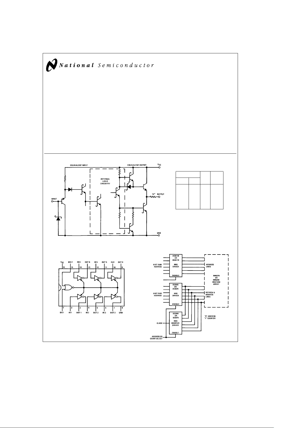
Schematic Diagram
*DS1649/DS3649 only TL/F/7515– 1
Truth Table
Disable Input
Input Output
DIS 1 DIS 2
0001
0010
0 1 X Hi-Z
1 0 X Hi-Z
1 1 X Hi-Z
XeDon’t care
Hi-Z
e
TRI-STATE mode
Connection Diagram
Dual-In-Line Package
TL/F/7515– 2
Top View
Order Number DS1649J, DS3649J,
DS1679J, DS3679J, DS3649N or DS3679N
See NS Package Number J16A or N16A
Typical Application
TL/F/7515– 3
C
1995 National Semiconductor Corporation RRD-B30M105/Printed in U. S. A.
Absolute Maximum Ratings (Note 1)
If Military/Aerospace specified devices are required,
please contact the National Semiconductor Sales
Office/Distributors for availability and specifications.
Supply Voltage 7.0V
Logical ‘‘1’’ Input Voltage 7.0V
Logical ‘‘0’’ Input Voltage
b
1.5V
Storage Temperature Range
b
65§Ctoa150§C
Maximum Power Dissipation* at 25§C
Cavity Package 1371 mW
Molded Package 1280 mW
Lead Temperature (Soldering, 10 sec.) 300
§
C
Operating Conditions
Min Max Units
Supply Voltage (V
CC
4.5 5.5 V
Temperature (T
A
)
DS1649, DS1679
b
55
a
125
§
C
DS3649, DS3679 0
a
70
§
C
*Derate cavity package 9.1 mW/§C above 25§C; derate molded package
10.2 mW/
§
C above 25§C.
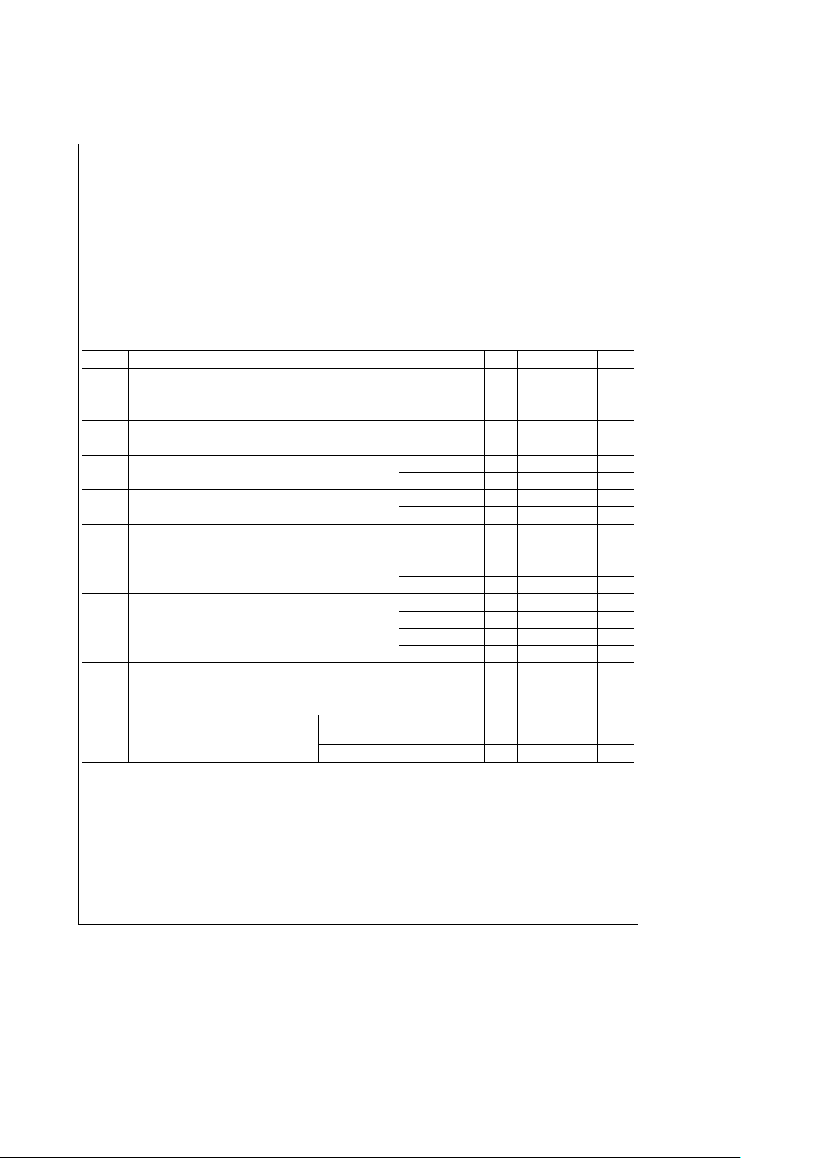
Electrical Characteristics (Note 2 and 3)
Symbol Parameter Conditions Min Typ Max Units
V
IN(1)
Logical ‘‘1’’ Input Voltage 2.0 V
V
IN(0)
Logical ‘‘0’’ Input Voltage 0.8 V
I
IN(1)
Logical ‘‘1’’ Input Current V
CC
e
5.5V, V
IN
e
5.5V 0.1 40 mA
I
IN(0)
Logical ‘‘0’’ Input Current V
CC
e
5.5V, V
IN
e
0.5V
b
50b250 mA
V
CLAMP
Input Clamp Voltage V
CC
e
4.5V, I
IN
eb
18 mA
b
0.75b1.2 V
V
OH
Logical ‘‘1’’ Output Voltage V
CC
e
4.5V, I
OH
eb
10 mA DS1649/DS1679 2.7 3.6 V
(No Load)
DS3649/DS3679 2.8 3.6
V
OL
Logical ‘‘0’’ Output Voltage V
CC
e
4.5V, I
OL
e
10 mA DS1649/DS1679 0.25 0.4 V
(No Load)
DS3649/DS3679 0.25 0.35 V
V
OH
Logical ‘‘1’’ Output Voltage V
CC
e
4.5V, I
OH
eb
1.0 mA DS1649 2.4 3.5 V
(With Load)
DS1679 2.5 3.5 V
DS3649 2.6 3.5 V
DS3679 2.7 3.5 V
V
OL
Logical ‘‘0’’ Output Voltage V
CC
e
4.5V, I
OL
e
20 mA DS1649 0.6 1.1 V
(With Load)
DS1679 0.4 0.5 V
DS3649 0.6 1.0 V
DS3679 0.4 0.5 V
I
1D
Logical ‘‘1’’ Drive Current V
CC
e
4.5V, V
OUT
e
0V (Note 4)
b
250 mA
I
0D
Logical ‘‘0’’ Drive Current V
CC
e
4.5V, V
OUT
e
4.5V (Note 4) 150 mA
Hi-Z TRI-STATE Output Current V
OUT
e
0.4V to 2.4V, DIS1 or DIS2e2.0V
b
40 40 mA
I
CC
Power Supply Current V
CC
e
5.5V One DIS Inpute3.0V
42 75 mA
All Other InputseX
All Inputse0V 11 20 mA
2
 Loading...