

NSC DM54123W-MIL, DM54123J-MIL Datasheet
March 1993
DM54123/DM74123 Dual Retriggerable One-Shot with
Clear and Complementary Outputs
DM54123/DM74123 Dual Retriggerable One-Shot with Clear and Complementary Outputs
General Description
The ’123 is a dual retriggerable monostable multivibrator
capable of generating output pulses from a few nano-seconds to extremely long duration up to 100% duty cycle.
Each device has three inputs permitting the choice of either
leading-edge or trailing edge triggering. Pin (A) is an activelow transition trigger input and pin (B) is an active-high transition trigger input. A low at the clear (CLR) input terminates
the output pulse: which also inhibits triggering. An internal
connection from CLR to the input gate makes it possible to
trigger the circuit by a positive-going signal on CLR as
shown in the truth table.
To obtain the best and trouble free operation from this device please read the operating rules as well as the NSC
one–shot application notes carefully and observe recommendations.
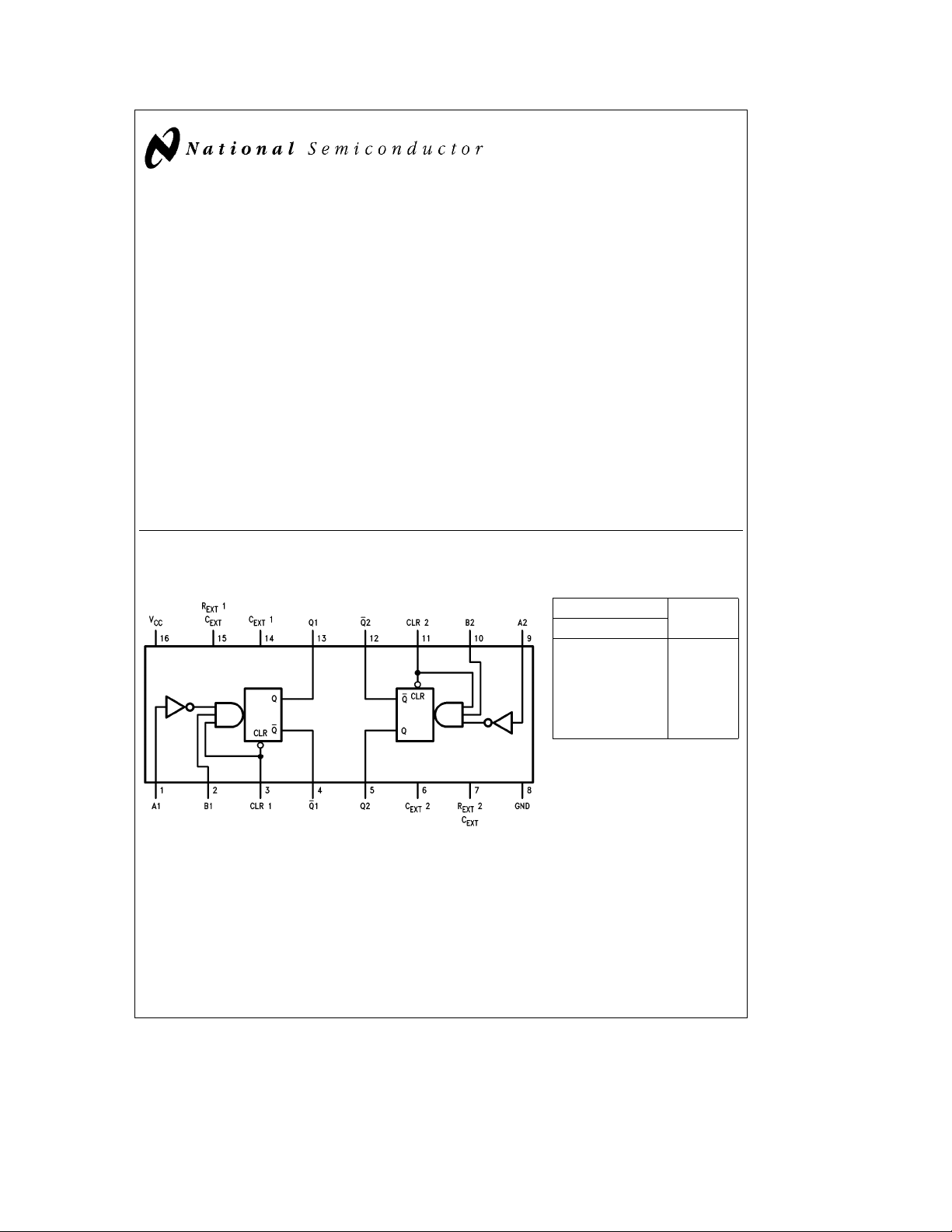
Connection Diagram
Dual-In-Line Package
Features
Y
DC triggered from active-high transition or active-low
transition inputs
Y
Retriggerable to 100% duty cycle
Y
Direct reset terminates output pulse
Y
Compensated for VCCand temperature variations
Y
DTL, TTL compatible
Y
Input clamp diodes
Functional Description
The basic output pulse width is determined by selection of
an external resistor (R
the basic pulse width may be extended by retriggering the
gated active-low transition or active-high transition inputs or
be reduced by use of the active-low transition clear input.
Retriggering to 100% duty cycle is possible by application of
an input pulse train whose cycle time is shorter than the
output cycle time such that a continuous ‘‘HIGH’’ logic state
is maintained at the ‘‘Q’’ output.
) and capacitor (CX). Once triggered,
X
Triggering Truth Table
Inputs
Response
A B CLR
X X L No Trigger
K L X No Trigger
K H H Trigger
H L X No Trigger
L L H Trigger
LHLTrigger
HeHIGH Voltage Level
e
LOW Voltage Level
L
e
Immaterial
X
Order Number DM54123J-MIL, DM54123W-MIL or DM74123N
TL/F/6539– 1
See NS Package Number J16A, N16A or W16A
C
1995 National Semiconductor Corporation RRD-B30M105/Printed in U. S. A.
TL/F/6539
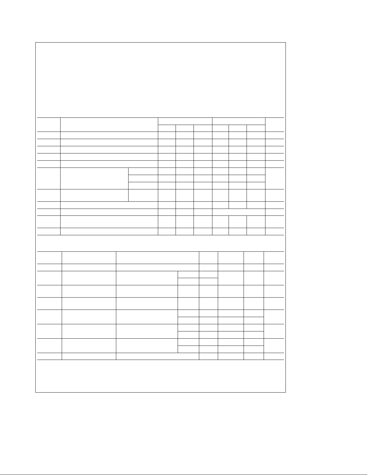
Absolute Maximum Ratings (Note)
If Military/Aerospace specified devices are required,
please contact the National Semiconductor Sales
Office/Distributors for availability and specifications.
Supply Voltage 7V
Input Voltage 5.5V
Operating Free Air Temperature Range
DM54
DM74 0
Storage Temperature
b
55§Ctoa100§C
Ctoa70§C
§
b
65§Ctoa150§C
Recommended Operating Conditions
Symbol Parameter
V
CC
V
IH
V
IL
I
OH
I
OL
t
W
T
WQ
(Min) Pulse at Q (Note 5)
R
EXT
C
EXT
C
WIRE
T
A
Supply Voltage 4.5 5 5.5 4.75 5 5.25 V
High Level Input Voltage 2 2 V
Low Level Input Voltage 0.8 0.8 V
High Level Output Current
Low Level Output Current 16 16 mA
Pulse Width A or B High 40
(Note 5)
A or B Low 40 ns
Clear Low 40
Minimum Width of A or B
External Timing Resistor 5 50 kX
External Timing Capacitance No Restriction mF
Wiring Capacitance
at R
EXT/CEXT
Terminal (Note 5)
Free Air Operating Temperature
The ‘‘Absolute Maximum Ratings’’ are those values
Note:
beyond which the safety of the device cannot be guaranteed. The device should not be operated at these limits. The
parametric values defined in the ‘‘Electrical Characteristics’’
table are not guaranteed at the absolute maximum ratings.
The ‘‘Recommended Operating Conditions’’ table will define
the conditions for actual device operation.
DM54123 DM74123
Min Nom Max Min Nom Max
b
0.8
b
0.8 mA
80 65 ns
50 pF
b
55 125 0 70
Units
C
§
Electrical Characteristics
over recommended operating free air temperature range (unless otherwise noted)
Symbol Parameter Conditions Min
e
V
I
V
OH
V
OL
I
I
I
IH
I
IL
I
OS
I
CC
Note 1: All typicals are at V
Note 2: Not more than one output should be shorted at a time.
Note 3: Quiescent I
25 KX.
Note 4: I
Note 5: T
Input Clamp Voltage V
High Level Output V
Voltage
Low Level Output V
Voltage V
Input Current@Max V
Input Voltage
High Level Input V
Current V
Low Level Input Current V
Short Circuit V
Output Current (Note 2)
Supply Current V
e
e
5V, T
CC
A
is measured (after clearing) with 2.4V applied to all clear and A inputs, B inputs grounded, all outputs open,C
CC
is measured in the triggered state with 2.4V applied to all clear and B inputs, A inputs grounded, all outputs open, C
CC
e
A
25§C and V
e
5V.
CC
25§C.
CC
CC
e
V
IL
CC
e
IH
CC
CC
e
I
CC
CC
CC
eb
Min, I
e
Min, I
Max, V
e
Min, I
Min, V
e
Max, V
e
Max Data 40
2.4V
e
Max, V
12 mA
I
e
Max DM54 2.4
OH
e
Min DM74 2.5
IH
e
Max
OL
e
Max
IL
e
5.5V
I
Clear 80
e
0.4V Clear
I
Data
e
Max DM54
DM74
e
Max (Notes 3 and 4) 46 66 mA
b
b
2
Typ
(Note 1)
Max Units
b
1.5 V
3.4 V
0.2 0.4 V
1mA
mA
b
3.2
b
1.6
e
EXT
e
0.02 mF, and R
b
b
0.02 mF, and R
10
10
EXT
mA
40
mA
40
e
EXT
e
25 kX.
EXT
 Loading...