NSC CLC409AMC, CLC409AJM5, CLC409AJE-TR13, CLC409AJE, CLC409AJ Datasheet
...
Features
■
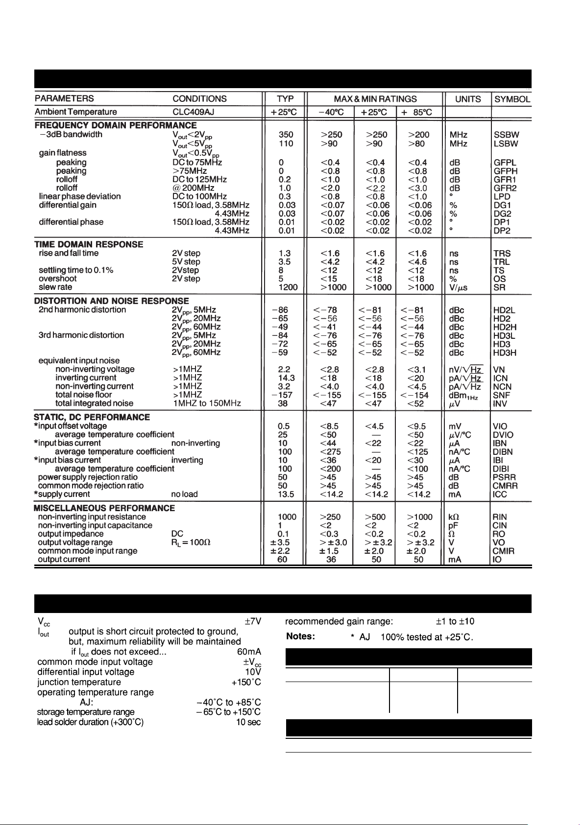
350MHz small signal bandwidth
■
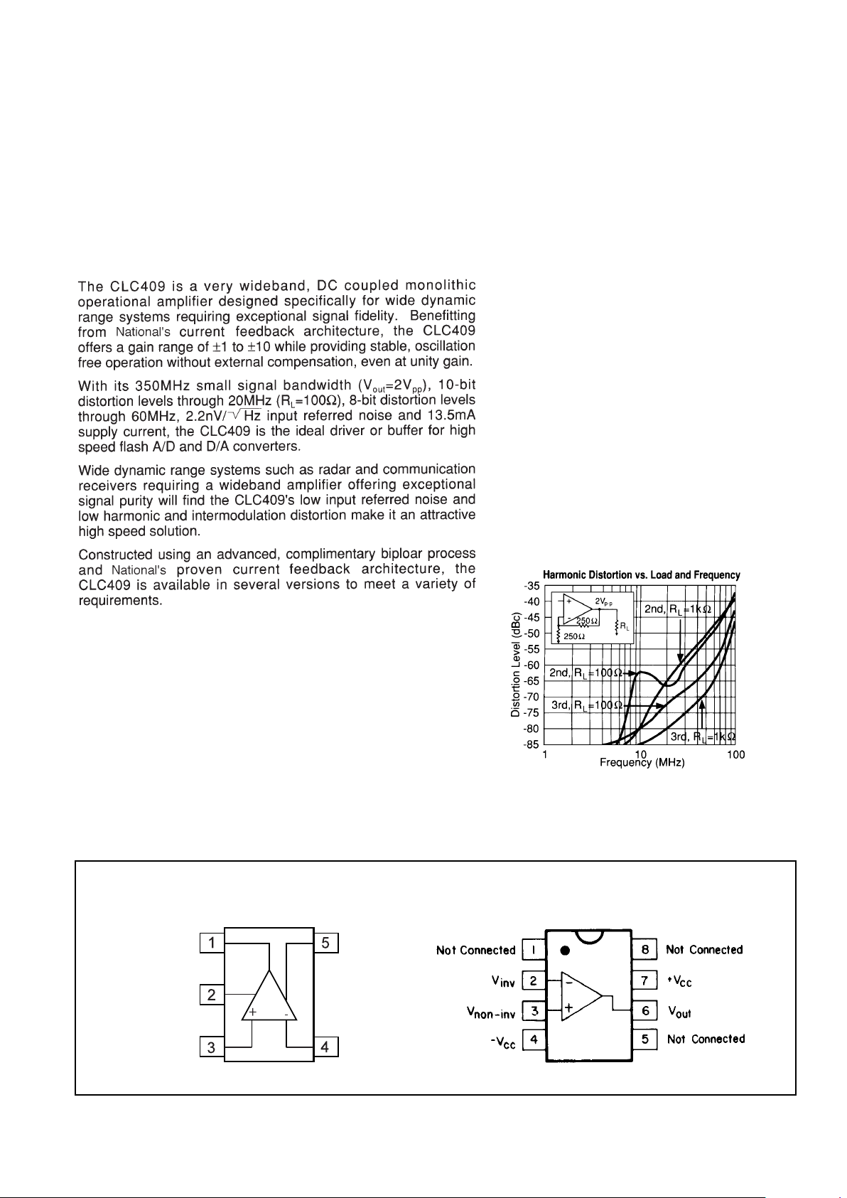
-65/-72dBc 2nd/3rd harmonics (20MHz)
■
Low noise
■
8ns settling to 0.1%
■
1200V/µs slew rate
■
13.5mA supply current (±5V)
■
70mA output current
Applications
■
Flash A/D driver
■
D/A transimpedance buffer
■
Wide dynamic range IF amp
■
Radar/communication receivers
■
DDS post-amps
■
Wideband inverting summer
■
Line driver
General Description
CLC409
Very Wideband, Low Distortion Monolithic Op Amp
N
June 1999
CLC409
Very Wideband, Low Distortion Monolithic Op Amp
© 1999 National Semiconductor Corporation http://www.national.com
Printed in the U.S.A.
CLC409AJP -40°C to +85°C 8-pin plastic DIP
CLC409AJE -40°C to +85°C 8-pin plastic SOIC
CLC409ALC -40°C to +85°C dice
CLC409AMC -55°C to +125°C dice qualified to Method 5008,
MIL-STD-883, Level B
CLC409AJM5 -40°C to +85°C 5-pin SOT
DESC SMD number: 5962-92034
Pinout
DIP & SOIC
V
inv
V
CC
V
EE
V
o
V
non-inv
Pinout
SOT23-5

CLC409 Electrical Characteristics
(Av= +2,Vcc= ±5V, RL= 100Ω,Rf= 250Ω; unless specified)
Absolute Maximum Ratings Miscellaneous Ratings
http://www.national.com 2
Min/max ratings are based on product characterization and simulation. Individual parameters are tested as noted. Outgoing quality levels are
determined from tested parameters.
EDS rating (human body model) 1000V
Pac kage Thermal Resistance
Package θ
JC
θ
JA
AJP 95°C/W 155°C/W
AJE 75°C/W 160°C/W
AJM5 115°C/W 185°C/W
Reliability Information
Transistor count 28
 Loading...