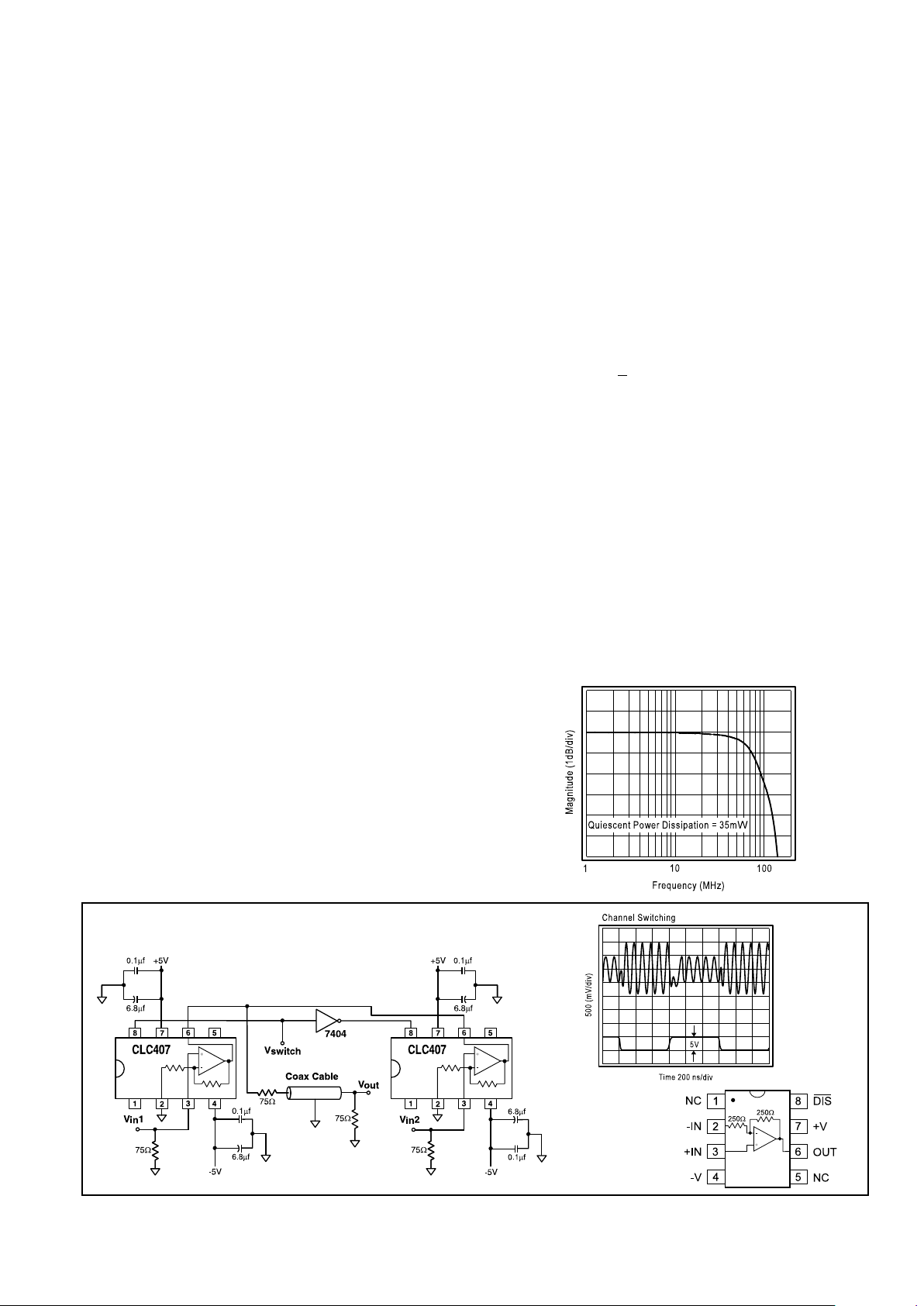
Frequency Response (AV = +2V/V)
Features
■
Low-cost
■
High output current: 60mA
■
High input impedance: 6MΩ
■
Gains of +1, +2 with no external components
■
Low power: Icc= 3.5mA
■
Ultra-fast enable/disable times
■
Very low input bias currents: 100nA
■
Excellent gain accuracy: 0.1%
■
High speed: 110MHz -3dB BW
Applications
■
Desktop video systems
■
Multiplexers
■
Video distribution
■
Flash A/D driver
■
High-speed switch/driver
■
High-source impedance applications
■
Peak detector circuits
■
Professional video processing
■
High resolution monitors
NOTE: All necessary components are shown.
Typical Application
2:1 Mux Cable Driver
Pinout
DIP & SOIC
General Description
The Comlinear CLC407 is a low-cost, high-speed (110MHz)
buffer which features user-programmable gains of +2, +1, and -1
V/V. This high-performance part has the added versatility of a
TTL-compatible disable which quickly switches the buffer off in
18ns and back on in 40ns. The CLC407’s high 60mA output
current, coupled with its ultra-low 35mW power consumption
makes it the ideal choice for demanding applications that are
sensitive to both power and cost.
Utilizing Comlinear’s proven architectures, this current feedback
amplifier surpasses the performance of alternate solutions with a
closed-loop design that produces new standards for buffers in
gain accuracy, input impedance, and input bias currents. The
CLC407’s internal feedback network provides an excellent gain
accuracy of 0.1%. High source impedance applications will
benefit from the CLC407’s 6MΩ input impedance along with its
exceptionally low 100nA input bias current.
With 0.1dB flatness to 30MHz and low differential gain and phase
errors, the CLC407 is very useful for professional video processing and distribution. A 110MHz -3dB bandwidth coupled with a
350V/µs slew rate also make the CLC407 a perfect choice in
cost-sensitive applications such as video monitors, fax machines,
copiers, and CATV systems. Back-terminated video applications
will especially appreciate +2 gains which require no external gain
components reducing inventory costs and board space.
Comlinear CLC407
Low-Cost, Low-Power
Programmable Gain Buffer with Disable
N
August 1996
Comlinear CLC407
Low-Cost, Low-Power, Programmable Gain Buffer with Disable
© 1996 National Semiconductor Corporation http://www.national.com
Printed in the U.S.A.

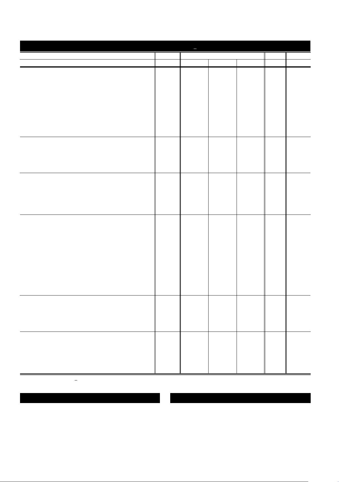
PARAMETERS CONDITIONS TYP MIN/MAX RATINGS UNITS NOTES
Ambient Temperature CLC407AJ +25˚C +25˚C 0 to 70˚C -40 to 85˚C
FREQUENCY DOMAIN RESPONSE
-3dB bandwidth V
out
< 1.0V
pp
110 75 50 45 MHz B
V
out
< 5.0V
pp
42 31 27 26 MHz 1
±
0.1dB bandwidth V
out
< 1.0V
pp
30 15 MHz
gain flatness V
out
< 1.0V
pp
peaking DC to 200MHz 0 0.4 0.6 0.8 dB B
rolloff <30MHz 0.1 0.5 0.65 0.7 dB B
linear phase deviation <20MHz 0.3 0.6 0.7 0.7 deg
differential gain NTSC, RL=150Ω 0.03 0.05 0.06 0.07 %
NTSC, RL=150Ω
(Note 2)
0.01 % 2
differential phase NTSC, RL=150Ω 0.25 0.4 0.5 0.55 deg
NTSC, RL=150Ω
(Note 2)
0.08 deg 2
TIME DOMAIN RESPONSE
rise and fall time 2V step 5 7.5 8.2 8.4 ns
settling time to 0.05% 2V step 18 27 36 39 ns
overshoot 2V step 3 12 12 12 %
slew rate AV = +2 2V step 350 260 225 215 V/µs
AV = -1 1V step 650 V/µs
DISTORTION AND NOISE RESPONSE
2nd harmonic distortion 2Vpp, 1MHz/10MHz -72/-52 -46 -45 -44 dBc B, C
3rd harmonic distortion 2V
pp
, 1MHz/10MHz -70/-57 -50 -47 -46 dBc B, C
equivalent input noise
non-inverting voltage >1MHz 5 6.3 6.6 6.7 nV/√Hz
inverting current >1MHz 12 15 16 17 pA/√Hz
non-inverting current >1MHz 3 3.8 4 4.2 pA/√Hz
STATIC DC PERFORMANCE
input offset voltage 1 5 7 8 mV
average drift 30 50 50 µV/˚C
input bias current non-inverting 100 900 1600 2800 nA A
average drift 3 8 11 nA/˚C
input bias current inverting 1 5 6 8 µA
average drift 17 40 45 nA/˚C
output offset voltage 2.5 13 17 19 mV A,3
amplifier gain error
±
0.1%
±
1.0%
±
1.0%
±
1.0% V/V A
internal feedback resistor (R
f
) 250
±
20% Ω
power supply rejection ratio DC 52 47 46 45 dB B
common-mode rejection ratio DC 50 45 44 43 dB
supply current R
L
= ∞ 3.5 4.0 4.1 4.4 mA A
disabled R
L
= ∞ 0.8 0.9 0.95 1 mA A
SWITCHING PERFORMANCE
turn on time 40 55 58 58 ns
turn off time to >50dB attn. @ 10MHz 18 26 30 32 ns
off isolation 10MHz 85 80 80 80 dB
high input voltage V
IH
222V
low input voltage V
IL
0.8 0.8 0.8 V
MISCELLANEOUS PERFORMANCE
input resistance non-inverting 6 3 2.4 1 MΩ
input capacitance non-inverting 1 2 2 2 pF
common mode input range ±2.2 1.8 1.7 1.5 V
output voltage range R
L
= ∞ +4.0,-3.3 +3.9,-3.2 +3.8,-3.1 +3.7,-2.8 V
output current 60 44 38 20 mA
output resistance, closed loop 0.06 0.2 0.25 0.4 Ω
Recommended gain range +1, +2 V/V
Min/max ratings are based on product characterization and simulation. Individual parameters are tested as noted. Outgoing quality levels are
determined from tested parameters.
CLC407 Electrical Characteristics
(AV= +2, Vcc= + 5V, RL= 100Ω unless specified)
Absolute Maximum Ratings
supply voltage
±
7V
I
out
is short circuit protected to ground
common-mode input voltage
±
Vcc
maximum junction temperature +175˚C
storage temperature range -65˚C to +150˚C
lead temperature (soldering 10 sec) +300˚C
Notes
1) At temps < 0˚C, spec is guaranteed for RL= 500Ω.
2) An 825Ω pull-down resistor is connected between V
o
and -Vcc.
3) Source impedance 1kΩ.
A) J-level: spec is 100% tested at +25˚C, sample tested at +85˚C.
LC/MC-level: spec is 100% wafer probed at +25˚C.
B)J-level: spec is sample tested at +25˚C.
C)Guaranteed at 10MHz.
http://www.national.com 2

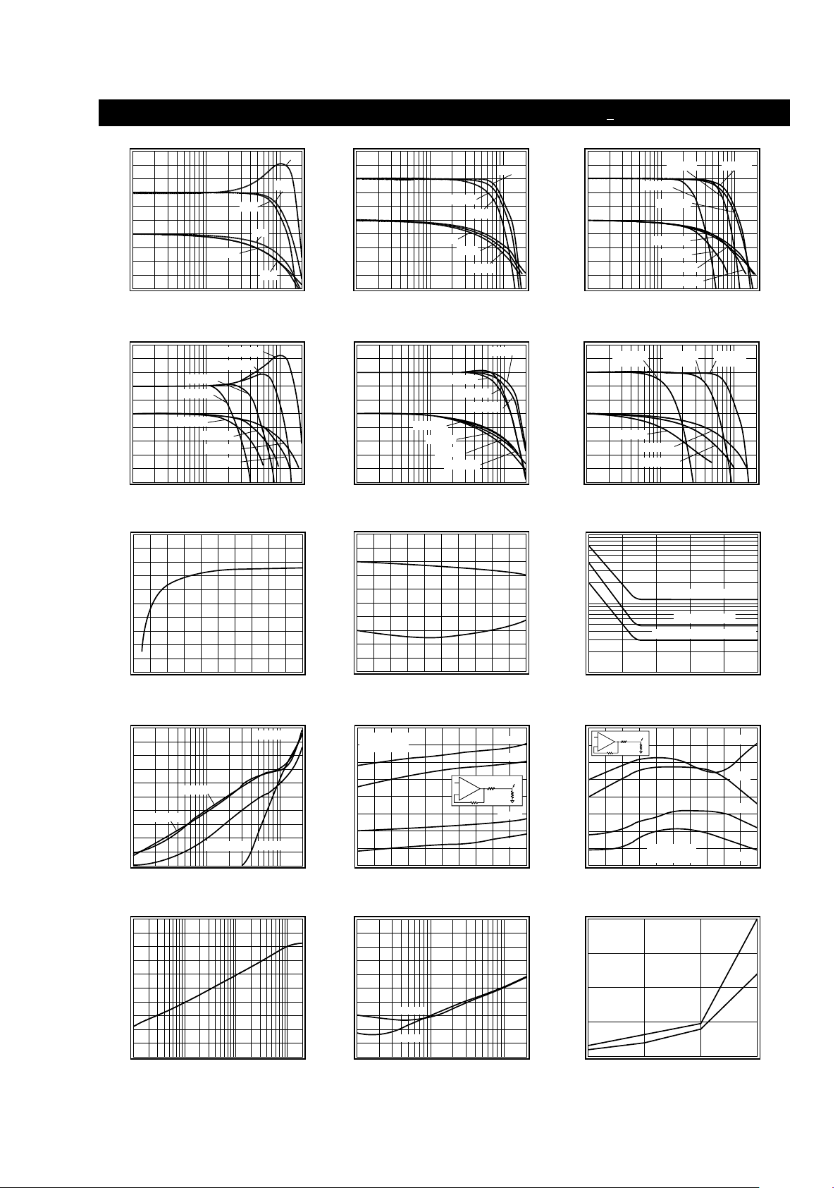
CLC407 Typical Performance Characteristics
(AV= +2, Rf= 250Ω: Vcc= + 5V, RL= 100Ω unless specified)
Frequency Response
Magnitude (1dB/div)
Phase (45
o
/div)
1
10
100
Frequency (MHz)
Gain
Phase
A
V
+2
A
V
+1
AV+1
AV-1
A
V
+2
AV -1
Frequency Response vs. R
L
Magnitude (1dB/div)
Phase (deg)
-180
-90
-135
-45
0
1
10
100
Frequency (MHz)
Gain
Phase
RL =50
RL =100
RL =1k
RL =50
RL =100
RL =1k
Frequency Response vs. V
out (Av
= +2)
Magnitude (1dB/div)
Phase (deg)
-180
-90
-135
-45
0
1
10
100
Frequency (MHz)
Gain
Phase
VO =1V
pp
VO =0.2V
pp
VO =5V
pp
VO =2V
pp
VO =5V
pp
VO =0.2V
pp
VO =1V
pp
VO =2V
pp
Frequency Response vs. V
out (Av
= +1)
Magnitude (1dB/div)
Phase (deg)
-180
-90
-135
-45
0
1
10
100
Frequency (MHz)
Gain
Phase
VO =1V
pp
VO =0.2V
pp
VO =2V
pp
VO =4V
pp
VO =2V
pp
VO =4V
pp
VO =1V
pp
VO =0.2V
pp
Frequency Response vs. V
out (Av
= -1)
Magnitude (1dB/div)
Phase (deg)
-360
-270
-315
-225
-180
1
10
100
Frequency (MHz)
Gain
Phase
VO =1V
pp
VO =0.2V
pp
VO =2V
pp
VO =4V
pp
VO =2V
pp
VO =4V
pp
VO =1V
pp
VO =0.2V
pp
Frequency Response vs. Capacitive Load
Magnitude (1dB/div)
Phase (deg)
-180
-90
-135
-45
0
1
10
100
Frequency (MHz)
Gain
Phase
CL =1kpF
Rs=10
CL =100pF
Rs= 30
CL =10pF
Rs=100
CL =1kpF
CL =100pF
CL =10pF
Maximum Output Voltage vs. R
L
Maximum Output Voltage (V
pp
)
Load (Ω)
7.0
6.0
5.0
4.0
3.0
2.0
1000200
300
400
500
Gain Flatness & Linear Phase Deviation
Magnitude (0.1dB/div)
LPD (0.5
o
/div)
0
15
30
Frequency (MHz)
Gain
Phase
Equivalent Input Noise
Noise Voltage (nV/√Hz)
Frequency (Hz)
100
10
1
1k
100
10k
100k
1M
10M
Noise Current (pA/√Hz)
100
10
1
Inverting Current = 12pA/√Hz
Voltage = 5nV/√Hz
Non-Inverting Current = 3pA/√Hz
2nd & 3rd Harmonic Distortion
Distortion (dBc)
Frequency (MHz)
-40
-50
-90
0.1
1
10
-70
-80
-60
3rd Rl = 100
2nd Rl = 1k
3rd Rl = 1k
2nd Rl = 100
Vo = 2V
pp
2nd Harmonic Distortion vs. P
out
Distortion (dBc)
Output Power (dBm)
-45
-55
-85
-10
0
10
-65
-75
500KHz
1MHz
5MHz
10MHz
10dBm = 2V
pp
0dBm = .63Vpp
+
-
50Ω
50Ω
Pout
3rd Harmonic Distortion vs. P
out
Distortion (dBc)
Output Power (dBm)
-45
-55
-85
-10
0
10
-65
-75
10dBm = 2V
pp
0dBm = .63Vpp
+
-
50Ω
50Ω
P
out
500KHz
1MHz
5MHz
10MHz
Output Resistance vs. Frequency
Output Resistance (20log Z
out
)
Frequency (MHz)
50
30
1
10
100
-10
-30
10
-50
Forward & Reverse Isolation During Disable
Gain (dB)
1
10
100
Frequency (MHz)
Forward
Reverse
-20
-40
-60
-80
-100
-120
Differential Gain & Phase
Differential Gain (%)
1
2
4
Number of 150Ω Loads
0.20
0.15
0.10
0.05
0
Differential Phase (deg)
1.00
0.75
0.50
0.25
0
Phase
Gain
3
3 http://www.national.com
