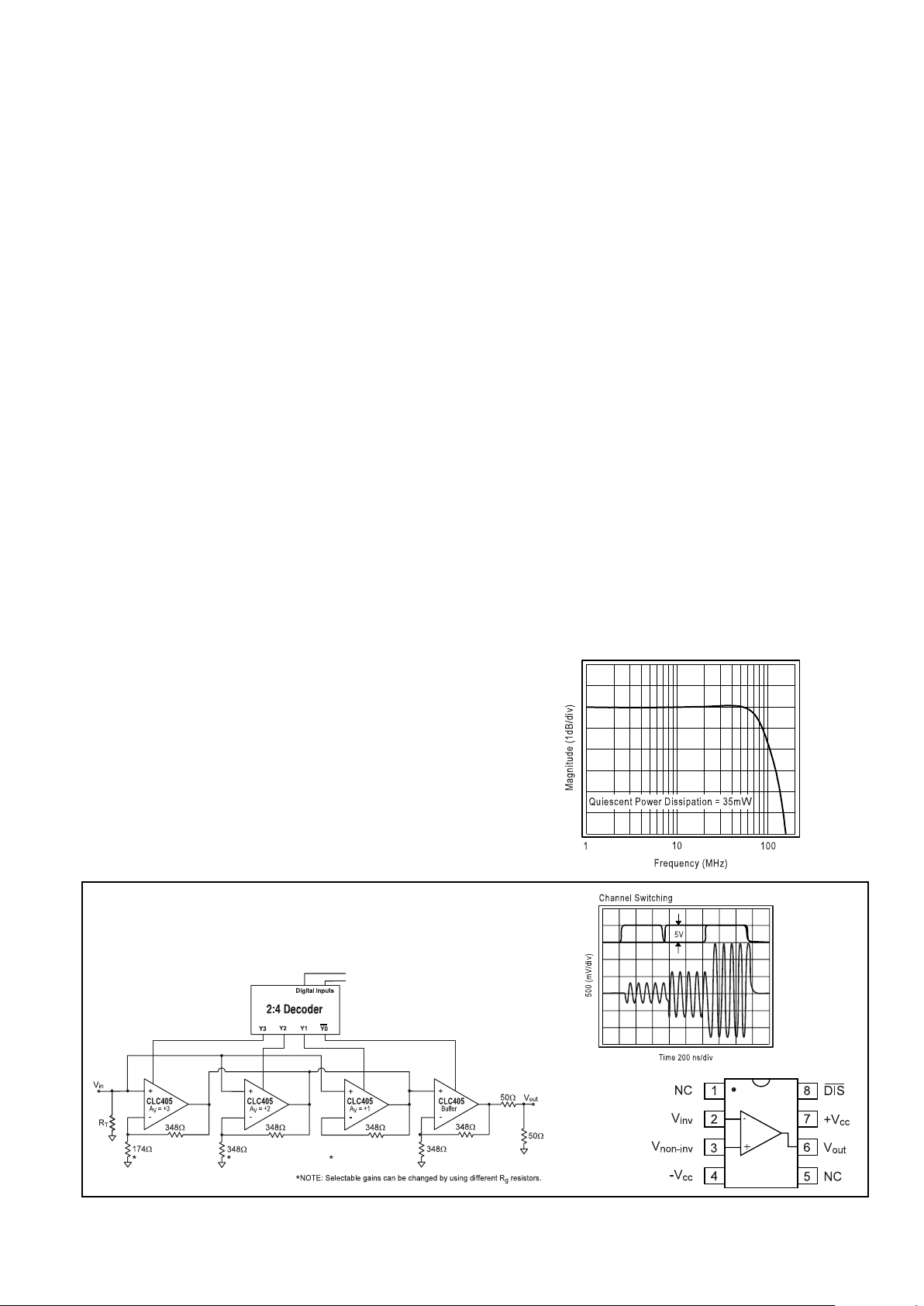
Frequency Response (Av = +2V/V)
Features
■
Low-cost
■
Very low input bias current: 100nA
■
High input impedance: 6MΩ
■
110MHz -3dB bandwidth (Av= +2)
■
Low power: Icc= 3.5mA
■
Ultra-fast enable/disable times
■
High output current: 60mA
Applications
■
Desktop video systems
■
Multiplexers
■
Video distribution
■
Flash A/D driver
■
High-speed switch/driver
■
High-source impedance applications
■
Peak detector circuits
■
Professional video processing
■
High resolution monitors
Typical Application
Wideband Digitally Controlled
Programmable Gain Amplifier
Pinout
DIP & SOIC
General Description
The CLC405 is a low-cost, wideband (110MHz) op amp featuring a TTL-compatible disable which quickly switches off in 18ns
and back on in 40ns. While disabled, the CLC405 has a very high
input/output impedance and its total power consumption drops to
a mere 8mW.When enabled, the CLC405 consumes only 35mW
and can source or sink an output current of 60mA. These
features make the CLC405 a versatile, high-speed solution for
demanding applications that are sensitive to both power and cost.
Utilizing National’s proven architectures, this current feedback
amplifier surpasses the performance of alternative solutions and
sets new standards for low power at a low price. This powerconserving op amp achieves low distortion with -72dBc and
-70dBc for second and third harmonics respectively. Many high
source impedance applications will benefit from the CLC405’s
6MΩ input impedance. And finally, designers will have a bipolar
part with an exceptionally low 100nA non-inverting bias current.
With 0.1dB flatness to 50MHz and low differential gain and phase
errors, the CLC405 is an ideal part for professional video
processing and distribution. However, the 110MHz -3dB bandwidth (Av= +2) coupled with a 350V/µs slew rate also make the
CLC405 a perfect choice in cost-sensitive applications such as
video monitors, fax machines, copiers, and CATV systems.
CLC405
Low-Cost, Low-Power, 110MHz Op Amp with Disable
N
June 1999
CLC405
Low-Cost, Low-Power, 110MHz Op Amp with Disable
© 1999 National Semiconductor Corporation http://www.national.com
Printed in the U.S.A.

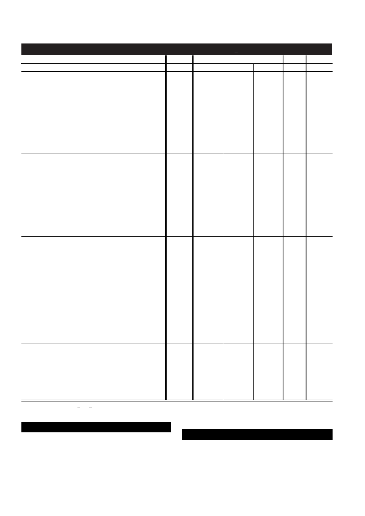
PARAMETERS CONDITIONS TYP MIN/MAX RATINGS UNITS NOTES
Ambient T emper ature CLC405AJ +25˚C +25˚C 0 to 70˚C -40 to 85˚C
FREQUENCY DOMAIN RESPONSE
-3dB bandwidth V
out
< 1.0V
pp
110 75 50 45 MHz
V
out
< 5.0V
pp
42 31 27 26 MHz 1
-3dB bandwidth A
V
= +1 V
out
< 0.5Vpp(Rf= 2K) 135 MHz
±
0.1dB bandwidth V
out
< 1.0V
pp
50 15 MHz
gain flatness V
out
< 1.0V
pp
peaking DC to 200MHz 0 0.6 0.8 1.0 dB
rolloff <30MHz 0.05 0.3 0.4 0.5 dB
linear phase deviation <20MHz 0.3 0.6 0.7 0.7 deg
differential gain NTSC, R
L
=150Ω 0.01 0.03 0.04 0.05 %
NTSC, R
L
=150Ω (Not e 2 ) 0.01 % 2
differential phase NTSC, R
L
=150Ω 0.25 0.4 0.5 0.55 deg
NTSC, R
L
=150Ω (Not e 2 ) 0.08 deg 2
TIME DOMAIN RESPONSE
rise and fall time 2V step 5 7.5 8.2 8.4 ns
settling time to 0.05% 2V step 18 27 36 39 ns
overshoot 2V step 3 12 12 12 %
slew rate A
V
= +2 2V step 350 260 225 215 V/µs
A
V
= -1 1V step 650 V/µs
DISTORTION AND NOISE RESPONSE
2
nd
harmonic distortion 2Vpp, 1MHz/10MHz -72/-52 -46 -45 -44 dBc B
3
rd
harmonic distortion 2Vpp, 1MHz/10MHz -70/-57 -50 -47 -46 dBc B
equivalent input noise
non-inverting voltage >1MHz 5 6.3 6.6 6.7 nV/√Hz
inverting current >1MHz 12 15 16 17 pA/√Hz
non-inverting current >1MHz 3 3.8 4 4.2 pA/√Hz
STATIC DC PERFORMANCE
input offset voltage 1 5 7 8 mV A
average drift 30 50 50 µV/˚C
input bias current non-inverting 100 900 1600 2800 nA A
average drift 3 8 11 nA/˚C
input bias current inverting 1 5 7 10 µAA
average drift 17 40 45 nA/˚C
power supply rejection ratio DC 52 47 46 45 dB
common-mode rejection ratio DC 50 45 44 43 dB
supply current R
L
= ∞ 3.5 4.0 4.1 4.4 mA A
disabled R
L
= ∞ 0.8 0.9 0.95 1 mA A
SWITCHING PERFORMANCE
turn on time 40 55 58 58 ns
turn off time to >50dB attn. @ 10MHz 18 26 30 32 ns
off isolation 10MHz 59 55 55 55 dB
high input voltage V
IH
222V
low input voltage V
IL
0.8 0.8 0.8 V
MISCELLANEOUS PERFORMANCE
input resistance non-inverting 6 3 2.4 1 MΩ
input resistance inverting 182 Ω
input capacitance non-inverting 1 2 2 2 pF
common mode input range
±
2.2 1.8 1.7 1.5 V
output voltage range R
L
= 100Ω + 3.5,-2.8 +3.1,-2.7 +2.9,-2.6 +2.4,-1.6 V
output voltage range R
L
= ∞ +4.0,-3.3 +3.9,-3.2 +3.8,-3.1 +3.7,-2.8 V
output current 40 40 38 20 mA
output resistance, closed loop 0.06 0.2 0.25 0.4 Ω
Recommended gain range +1 to +40V/V
Min/max ratings are based on product characterization and simulation. Individual parameters are tested as noted. Outgoing quality levels are
determined from tested parameters.
CLC405 Electrical Characteristics
(AV= +2, Rf= 348Ω:Vcc= + 5V, RL= 100Ω unless specified)
Absolute Maximum Ratings
supply voltage
±
7V
I
out
is short circuit protected to ground
common-mode input voltage
±
Vcc
maximum junction temperature +150˚C
storage temperature range -65˚C to +150˚C
lead temperature (soldering 10 sec) +300˚C
Notes
1) At temps < 0˚C, spec is guaranteed for RL= 500Ω.
2) An 825Ω pull-down resistor is connected between
V
o
and -Vcc.
A) J-level:spec is 100% tested at +25˚C
B)Guaranteed at 10MHz.
http://www.national.com 2
Transitor count 68
 Loading...